What Is a Low Loss PCB?
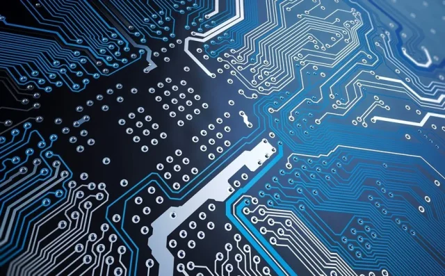
A Low Loss PCB is a printed circuit board engineered to reduce signal attenuation, insertion loss, and distortion during high-speed or high-frequency signal transmission. Low loss PCBs are essential in applications such as 5G communication, mmWave modules, data centers, automotive radar, and AI servers, where signal integrity is critical.
Compared with standard FR-4 PCBs, Low Loss PCBs use specialized laminate materials, smooth copper foils, and precise manufacturing processes to achieve superior electrical performance.
Key Characteristics of Low Loss PCB
A reliable Low Loss PCB typically features:
-
Low dissipation factor (Df)
Minimizes dielectric loss at high frequencies. -
Stable dielectric constant (Dk)
Ensures consistent impedance control. -
Smooth copper surface
Reduces conductor loss due to skin effect. -
Tight impedance tolerance
Essential for high-speed and RF signal paths. -
High thermal stability
Supports high-power and lead-free assembly.
These characteristics directly impact signal integrity and system performance.
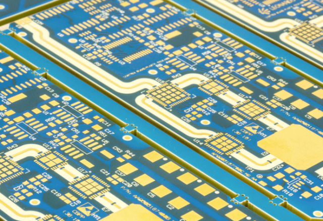
Low Loss PCB Material Options
Common materials used for Low Loss PCB fabrication include:
-
Panasonic Megtron 6 / Megtron 7
Ultra-low loss materials for high-speed digital designs. -
Rogers RO4350B / RO4003C
Widely used in RF and microwave applications. -
Taconic RF-35 / RF-60A
Cost-effective low-loss RF laminates. -
PTFE-based materials (RT/duroid series)
Ultra-low loss for mmWave applications. -
Hybrid PCB stack-ups
Combine low-loss and standard materials for optimized cost and performance.
Material selection depends on frequency, data rate, and application requirements.
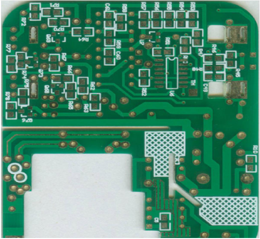
Design Considerations for Low Loss PCB
Effective Low Loss PCB design requires:
-
Optimized stack-up design
Short signal paths and controlled impedance layers. -
Differential pair tuning
Ensures minimal skew and loss. -
Via optimization and back drilling
Reduces via stubs and reflections. -
Proper grounding and shielding
Controls EMI and crosstalk. -
Thermal design integration
Maintains stable electrical performance.
Close collaboration between design and manufacturing teams is essential.
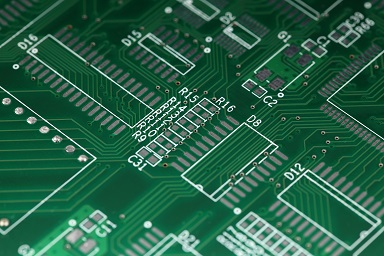
Manufacturing Challenges of Low Loss PCB
Producing a Low Loss PCB involves advanced manufacturing challenges:
-
Fine line and spacing control
-
Strict impedance tolerance
-
Copper roughness management
-
Precise lamination and registration
-
Advanced inspection and electrical testing
Even small process variations can affect low-loss performance.
Applications of Low Loss PCB
Low Loss PCBs are widely used in:
-
5G and mmWave communication equipment
-
High-speed routers and switches
-
AI servers and data center hardware
-
Automotive radar and ADAS systems
-
High-frequency test and measurement equipment
-
Semiconductor test boards
They are critical for next-generation electronics.
Conclusion
A Low Loss PCB is essential for high-speed and high-frequency electronic systems where signal integrity and performance are critical. By using advanced materials, precise design techniques, and controlled manufacturing processes, Low Loss PCBs deliver stable, reliable, and high-performance signal transmission.
Choosing an experienced Low Loss PCB manufacturer ensures optimized material selection, accurate impedance control, and consistent quality from prototype to mass production.
