A Low Loss PCB is a specialized printed circuit board engineered to reduce signal attenuation, dielectric loss, and insertion loss in high-speed and high-frequency electronic systems. As data rates and operating frequencies continue to increase, conventional PCB materials can no longer meet performance requirements, making low loss PCB technology essential for modern electronics.
Low loss PCBs are widely used in 5G communication, RF and microwave systems, high-speed digital backplanes, semiconductor test boards, automotive radar, and aerospace electronics, where signal integrity is critical.
Key Characteristics of Low Loss PCB Technology

1. Low Dielectric Loss Materials
Low loss PCBs utilize advanced laminates such as Rogers, PTFE, low-Dk/low-Df materials, and hybrid stackups to minimize dielectric loss and preserve signal quality at high frequencies.
2. Controlled Impedance and Precision Routing
Accurate controlled impedance routing ensures stable signal transmission, reducing reflections, jitter, and eye-diagram degradation in high-speed and RF circuits.
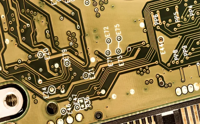
3. Optimized Multilayer Stackups
Low loss PCBs often adopt carefully designed multilayer stackups with dedicated ground and power planes to reduce EMI, crosstalk, and signal loss.
4. Smooth Copper and Surface Treatment
Using low-profile or reverse-treated copper foils minimizes conductor loss caused by skin effect, improving performance at gigahertz frequencies.
5. High-Frequency Signal Integrity
Low loss PCB design focuses on short signal paths, controlled trace geometry, and precise impedance matching to ensure consistent high-frequency performance.
Applications of Low Loss PCBs
Low loss PCBs are widely applied in:
-
5G base stations and mmWave communication systems
-
RF front-end modules and microwave circuits
-
High-speed digital servers and networking equipment
-
Automotive radar and ADAS systems
-
Semiconductor test PCBs (ATE, load boards, probe cards)
-
Aerospace and defense electronics
These applications demand minimal signal degradation, high reliability, and repeatable electrical performance.
Manufacturing Requirements for Low Loss PCBs
Producing high-quality low loss PCBs requires:
-
Advanced low-loss laminate processing capability
-
Precise lamination and registration control
-
Fine-line etching and impedance verification
-
Strict control of surface roughness and copper quality
-
Support for prototype, small batch, and volume production
Consistent manufacturing ensures stable electrical properties and long-term performance reliability.
Why Low Loss PCB Quality Matters

Inferior low loss PCBs can lead to:
-
Excessive signal attenuation and phase distortion
-
Reduced RF efficiency and data transmission speed
-
Inaccurate test results in semiconductor validation
-
Increased system noise and EMI issues
A professionally manufactured Low Loss PCB ensures clean signal transmission, accurate measurements, and optimal system performance.
Conclusion
The Low Loss PCB is a critical foundation for high-speed and high-frequency electronic systems. By combining low dielectric loss materials, controlled impedance routing, optimized multilayer design, and advanced manufacturing processes, low loss PCBs deliver superior signal integrity and reliable performance.
Choosing an experienced low loss PCB manufacturer enables faster product development, higher system efficiency, and long-term operational reliability in demanding applications.
