Low Loss Materials are a foundational requirement in modern PCB design where signal integrity, insertion loss, and timing accuracy directly determine system performance. As data rates increase and operating frequencies extend into multi-GHz and mmWave ranges, dielectric loss transitions from a secondary concern to a primary limiting factor in electronic system design.
Why Low Loss Materials Matter at High Frequency
At low frequencies, conductor resistance dominates signal degradation. However, as frequency increases, dielectric polarization loss becomes a major contributor to attenuation and phase distortion. Conventional FR-4 materials exhibit rising loss tangent and dielectric instability under these conditions, limiting achievable bandwidth and link margin.
Low Loss Materials are selected when:
-
Channel loss budget is tightly constrained
-
Signal eye opening is sensitive to attenuation
-
Phase delay consistency impacts system timing
-
Equalization alone cannot compensate for material-induced loss
In these scenarios, material performance directly defines system feasibility.
Electrical Characteristics That Define Low Loss Materials
From an electromagnetic perspective, Low Loss Materials are characterized by low dissipation factor (Df) and stable dielectric constant (Dk) over frequency and temperature. These properties influence how energy propagates and dissipates within the dielectric medium.
Key electrical behaviors include:
-
Reduced dielectric contribution to insertion loss
-
Stable impedance across operating bandwidth
-
Lower phase distortion and group delay variation
-
Improved correlation between simulation and measurement
This electrical stability is essential for predictable high-speed and RF design.
Impact on Signal Integrity and Timing
In high-speed digital and RF systems, signal degradation is cumulative. Even small reductions in dielectric loss can produce measurable improvements in system margins.
Low Loss Materials contribute to:
-
Cleaner eye diagrams at high data rates
-
Reduced jitter caused by dielectric dispersion
-
Improved channel-to-channel matching
-
Enhanced phase coherence in RF paths
These advantages are especially important in backplanes, SerDes links, RF front ends, and mixed-signal systems.
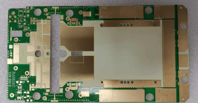
Thermal and Mechanical Considerations
Low Loss Materials often rely on PTFE, hydrocarbon-ceramic, or modified epoxy resin systems. While electrically superior, these materials introduce mechanical and thermal considerations that must be managed through design.
Engineering trade-offs include:
-
Managing coefficient of thermal expansion (CTE)
-
Ensuring copper adhesion during thermal cycling
-
Maintaining dimensional stability in multilayer stackups
-
Balancing rigidity with electrical performance
Effective stackup design aligns electrical requirements with mechanical reliability.
Manufacturing Consistency and Process Control
The benefits of Low Loss Materials can only be realized through disciplined manufacturing control. Variations in laminate thickness, resin content, or lamination pressure can directly impact impedance and loss performance.
Critical process controls include:
-
Tight dielectric thickness tolerance
-
Controlled lamination profiles
-
Precision drilling and copper plating
-
Electrical testing focused on impedance and loss
A capable PCB supplier integrates material behavior into manufacturing process planning.
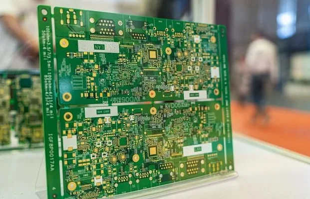
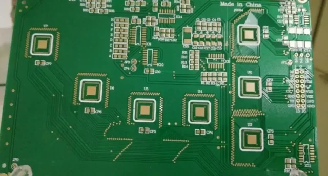
Typical Applications of Low Loss Materials
Low Loss Materials are widely applied in:
-
High-speed digital backplanes and interconnects
-
RF and microwave communication systems
-
5G and mmWave infrastructure
-
Data center networking hardware
-
Test and measurement equipment
In these applications, Low Loss Materials enable higher data rates, longer trace lengths, and improved system robustness.
Engineering Perspective
Low Loss Materials should be treated as electromagnetic performance enablers, not commodity laminates. Their selection influences loss budget, timing accuracy, and overall system reliability. When combined with controlled impedance stackups and manufacturing discipline, Low Loss Materials unlock performance levels unattainable with standard PCB substrates.
KKPCB supports Low Loss Material projects through material selection guidance, impedance-driven stackup engineering, and high-frequency process control, ensuring consistent electrical performance across production.
