Hybrid PCB materials are engineered by combining multiple laminate systems within a single PCB stackup to meet diverse electrical, thermal, and mechanical requirements. As electronic systems increasingly integrate high-speed digital, RF, and power circuitry on one board, no single material can simultaneously optimize all performance parameters. Hybrid PCB materials provide a practical engineering solution to this limitation.
Why Hybrid PCB Materials Are Necessary
Different functional blocks impose different material demands:
-
High-speed digital signals require low-loss, impedance-stable dielectrics
-
RF and microwave sections demand extremely low dissipation factor and dielectric consistency
-
Power circuits need high TG, high thermal stability, and mechanical robustness
Hybrid PCB materials allow designers to place low-loss laminates, high TG materials, and thermal substrates exactly where they are needed, enabling optimized performance without overdesign.
Electrical Performance and Signal Integrity
Hybrid PCB designs significantly improve signal integrity by:
-
Maintaining controlled impedance across mixed-material regions
-
Reducing insertion loss and reflection in high-speed channels
-
Isolating sensitive RF traces from noisy power planes
-
Minimizing crosstalk in dense multilayer stackups
Through careful material transition design and impedance modeling, hybrid PCB materials ensure predictable high-frequency performance even in complex routing environments.
Thermal Management and Power Density
Thermal performance is a major driver for hybrid PCB materials. By integrating:
-
High TG materials in power-dense zones
-
Thermally stable substrates under heat-generating components
-
Low-loss laminates in signal-critical layers
Hybrid PCBs effectively manage heat while maintaining electrical stability. This approach reduces thermal stress, limits board warpage, and extends product lifespan in high-power electronic systems.
Mechanical Reliability and Stackup Engineering
Combining different materials introduces challenges in CTE matching, lamination compatibility, and via reliability. Successful hybrid PCB design requires:
-
Precise stackup symmetry to prevent warpage
-
Controlled resin flow during lamination
-
Optimized via structures across material boundaries
-
Strict thickness and registration control
When properly engineered, hybrid PCB materials deliver long-term mechanical reliability comparable to single-material designs.
Manufacturing Considerations
From a fabrication perspective, hybrid PCB materials demand:
-
Advanced lamination process control
-
Material-specific drilling and via formation parameters
-
Careful impedance verification across layers
-
Enhanced inspection and electrical testing
An experienced PCB manufacturer ensures that performance gains are not compromised by manufacturability issues, enabling stable volume production.
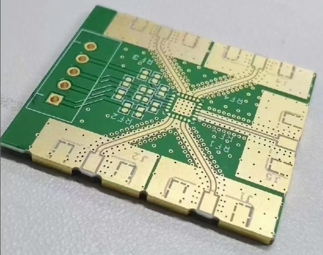
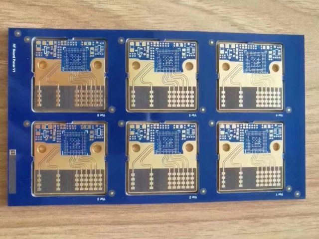
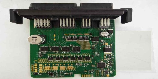
Typical Applications
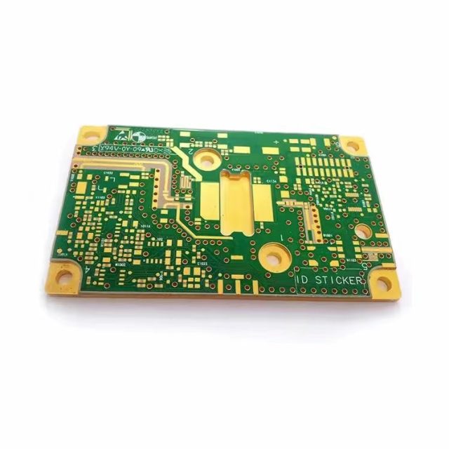
Hybrid PCB materials are widely used in:
-
5G base stations and RF front-end modules
-
High-speed networking and data center hardware
-
Power electronics with integrated control logic
-
Aerospace and defense electronics
-
Industrial automation and high-reliability systems
In these applications, hybrid PCBs provide a balanced platform for electrical performance, thermal control, and mechanical strength.
Engineering Perspective
Hybrid PCB materials represent a design philosophy rather than a material choice. By strategically combining material systems, engineers achieve optimized performance at the system level. With proper stackup design and manufacturing discipline, hybrid PCBs enable advanced electronic architectures that would be impractical using a single laminate.
KKPCB supports hybrid PCB projects with material selection consulting, stackup optimization, impedance control, and precision manufacturing, ensuring performance consistency from prototype to volume production.
