As data rates continue to increase across modern electronics, validating high-speed signals becomes more challenging. The High Speed Test PCB provides a stable and repeatable platform for evaluating signal integrity, timing, and performance in high-speed digital and mixed-signal systems.
High speed test PCBs are essential for accurate measurement and debugging.
What Is a High Speed Test PCB?
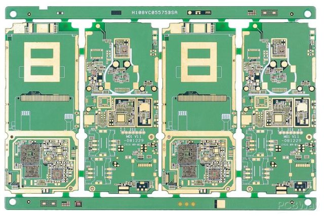
A High Speed Test PCB is a specialized printed circuit board designed to support high-speed signal testing, typically involving multi-gigabit data rates, fast edge transitions, and tight timing margins.
These PCBs are engineered to minimize loss, distortion, and noise during testing.
Key Design Challenges in High Speed Test PCBs
High speed test PCB design must address:
-
Controlled impedance routing
-
Crosstalk and electromagnetic interference (EMI)
-
Signal reflection and insertion loss
Each challenge directly impacts test accuracy.
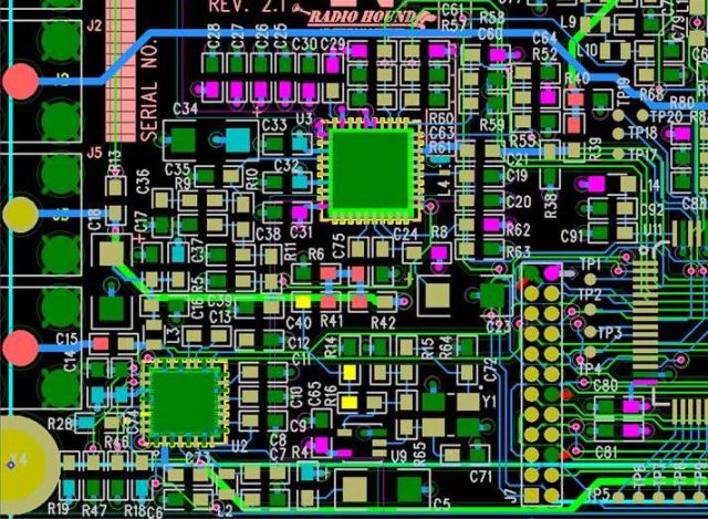
Signal Integrity Optimization
Maintaining signal integrity is the primary goal of a high speed test PCB. Key strategies include:
-
Precise impedance control
-
Short and matched trace lengths
-
Proper reference plane design
These measures preserve waveform fidelity.
Power Integrity for High-Speed Testing
High-speed circuits are sensitive to power noise. High speed test PCBs incorporate:
-
Robust power and ground plane structures
-
Optimized decoupling capacitor placement
-
Low-inductance current paths
Stable power improves test repeatability.
Stackup and Material Selection
Material choice is critical for high speed test PCBs. Designers often use:
-
Low-loss dielectric materials
-
Carefully planned multilayer stackups
-
Symmetrical layer constructions
These decisions reduce signal degradation.
Manufacturing Precision and Quality Control
High speed test PCBs require:
-
Tight fabrication tolerances
-
Accurate layer alignment
-
Comprehensive impedance and electrical testing
Manufacturing quality directly affects performance.
Typical Applications of High Speed Test PCBs
High speed test PCBs are widely used in:
-
SerDes and high-speed digital validation
-
Interface testing (PCIe, USB, Ethernet)
-
Semiconductor device characterization
-
ATE and lab test platforms
Each application benefits from controlled signal behavior.
Choosing a High Speed Test PCB Manufacturer
When selecting a high speed test PCB supplier, consider:
-
Experience with high-speed and test PCBs
-
Controlled impedance and SI expertise
-
Advanced multilayer manufacturing capability
-
Engineering support for design optimization
A qualified partner ensures reliable results.
Conclusion
The High Speed Test PCB is a critical tool for validating modern high-speed electronics. By ensuring controlled impedance, stable power delivery, and precise manufacturing, high speed test PCBs enable accurate signal measurement and confident system validation.
Partnering with an experienced high speed test PCB manufacturer ensures consistent performance across engineering and production test environments.
