As modern electronics become faster, more compact, and more data-intensive, the High Speed PCB has evolved into a critical engineering platform for communication systems, servers, AI accelerators, radar units, embedded computing modules, and advanced industrial electronics. A well-engineered High Speed PCB ensures clean signal transmission, stable power behavior, and low-jitter operation across multi-gigabit channels.
High-speed failures—reflections, crosstalk, jitter, mode conversion, power noise—often originate from PCB layout errors rather than component quality. Therefore, the High Speed PCB is not simply a board; it is a highly tuned transmission system engineered with precision electromagnetic principles.
1. What Defines a High Speed PCB?
A High Speed PCB carries signals where the physical PCB trace behaves as a transmission line, typically:
-
≥ 500 Mbps (high-speed digital)
-
≥ 1 GHz (RF and high-frequency communication)
-
Multi-gigabit interfaces such as PCIe, USB 3.x, SERDES, MIPI, HDMI, LVDS
At these speeds, the primary engineering challenge becomes Signal Integrity (SI) and Power Integrity (PI) rather than component placement alone.
2. Core Engineering Principles of High Speed PCB

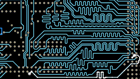
2.1 Controlled Impedance & Transmission Lines
Every High Speed PCB must maintain precise impedance, typically:
-
50Ω single-ended
-
85Ω or 90Ω differential for USB, HDMI, PCIe, LVDS
Engineering methods include:
-
Consistent dielectric thickness
-
Uniform trace width/spacing
-
Tight copper roughness control
-
Material Dk stability across temperature
Impedance accuracy determines whether signals propagate cleanly or degrade.
2.2 Differential Pair Engineering
High Speed PCB performance is heavily dependent on differential pair routing:
-
Tight pair spacing
-
Precise length matching
-
Phase alignment
-
Good reference plane continuity
-
Symmetrical return-path design
Any mismatch introduces skew, jitter, and data corruption at high data rates.
2.3 Crosstalk Mitigation
In high-density routing, crosstalk is one of the biggest threats.
High Speed PCB design requires:
-
Increasing spacing between sensitive signal groups
-
Using stripline over microstrip for better isolation
-
Applying ground shielding traces
-
Utilizing stacked reference planes
Crosstalk directly impacts signal fidelity at very high frequencies.
2.4 Return Path Control
Every high-speed signal must have a clean, continuous return path.
Therefore, a High Speed PCB must include:
-
Uninterrupted reference planes
-
Stitching vias for layer transitions
-
Eliminating splits and gaps under critical traces
-
Controlled electromagnetic field containment
Return-path discontinuities are a common cause of EMI radiation and signal distortion.
3. High-Speed Power Integrity (PI) Engineering
A High Speed PCB requires a stable, noise-free power system:
-
Decoupling networks tuned to target PDN impedance
-
Localized capacitors for high transient loads
-
Low-inductance mounting strategies
-
Multiple power/ground vias
-
Optimized plane resonance management
Poor PI results in jitter and timing collapse on high-speed interfaces.
4. Material Selection for High Speed PCB
The dielectric material determines loss, impedance stability, and high-frequency performance.
Common materials:
-
Rogers 4350B / 4003C
-
Panasonic Megtron 6 / 7
-
Isola I-Tera MT40
-
Taconic RF laminates
-
Low-Dk/low-loss FR-4 (limited applications)
The right material enables low-loss propagation across multi-gigabit channels.
5. High Speed PCB Stackup Engineering
Stackup is the skeleton of every High Speed PCB.
A typical configuration:
-
Dedicated ground reference layers
-
Controlled-impedance stripline layers
-
Power distribution plane with low-inductance return
-
Isolation layers to reduce EMI
-
Balanced mechanical symmetry
Advanced applications often require 8–16 layers to support dense routing and precision SI/PI optimization.
6. High-Speed Validation and Testing
A High Speed PCB undergoes rigorous testing:
-
TDR (Time Domain Reflectometry)
-
VNA for S-parameters
-
Eye diagram analysis
-
Crosstalk and jitter measurement
-
High-speed SERDES compliance testing
-
Thermal cycling and reliability screening
Only after passing SI/PI validation can a High Speed PCB function reliably in mission-critical systems.
Engineering Summary
The High Speed PCB is fundamental to next-generation electronics, enabling:
-
High-bandwidth communication
-
Ultra-low-latency computing
-
Radar and RF applications
-
Embedded AI systems
-
Autonomous platforms
-
Server-grade and networking hardware
From controlled impedance and differential routing to stackup design and material science, the engineering of a High Speed PCB requires deep expertise and precision manufacturing.
KKPCB specializes in complex, multilayer High Speed PCB fabrication and engineering, delivering highly reliable boards for advanced digital, RF, and high-speed applications.
