High Frequency Signal PCB: Design Principles for Reliable RF and High-Speed Applications
With the rapid development of wireless communication, radar systems, and high-speed digital electronics, High Frequency Signal PCB design has become increasingly critical. Signals operating in the GHz range are highly sensitive to impedance mismatches, dielectric loss, electromagnetic interference (EMI), and routing discontinuities. Therefore, designing a reliable high-frequency PCB requires careful consideration of materials, stackup architecture, and signal integrity.
This article explores the key design principles, materials, and manufacturing considerations for High Frequency Signal PCBs, helping engineers achieve stable performance in RF and high-speed applications.
What Is a High Frequency Signal PCB?
A High Frequency Signal PCB is a printed circuit board designed to transmit signals at high frequencies, typically above 500 MHz and often extending into the multi-GHz range. These PCBs are optimized to minimize signal loss, maintain controlled impedance, and ensure stable signal transmission.
High frequency signal PCBs are commonly used in:
-
RF communication modules
-
Microwave circuits
-
5G base stations
-
Radar systems
-
Satellite communication devices
-
High-speed networking equipment
Because signal behavior changes significantly at higher frequencies, specialized materials and design techniques are required.
Key Design Considerations for High Frequency Signal PCB
1. Controlled Impedance Design
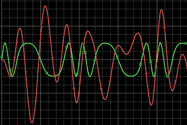
Maintaining consistent controlled impedance is essential for high-frequency signal transmission. Trace width, dielectric thickness, and copper weight must be carefully calculated to match the required impedance values, typically 50Ω or 75Ω for RF circuits.
2. Low-Loss PCB Materials
Material selection plays a major role in high-frequency PCB performance. Standard FR-4 materials may introduce excessive dielectric loss at GHz frequencies. Advanced laminates such as those produced by Rogers Corporation provide lower loss and better signal stability.
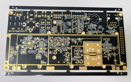
3. Optimized PCB Stackup
A well-designed high-frequency PCB stackup improves signal integrity and EMI control. Typical stackup strategies include:
-
Dedicated ground planes for RF signals
-
Short signal return paths
-
Symmetrical multilayer PCB structures
These design techniques help maintain signal integrity and reduce noise.
4. Short and Direct Signal Routing
High-frequency signals are more susceptible to reflections and attenuation. Designers should minimize trace length, avoid unnecessary vias, and maintain smooth routing transitions.
5. Grounding and Shielding
Effective grounding and shielding techniques reduce electromagnetic interference and improve RF signal quality. Continuous ground planes and via stitching are commonly used in high-frequency PCB layouts.
Materials Used in High Frequency Signal PCB
Several specialized materials are commonly used in high-frequency PCBs, including:
-
PTFE-based laminates
-
Hydrocarbon ceramic laminates
-
Low-loss epoxy materials
-
High-frequency Rogers laminates
These materials provide stable dielectric constants and low dissipation factors, enabling reliable performance at high frequencies.
Applications of High Frequency Signal PCB
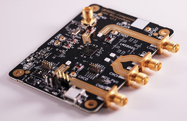
High-frequency signal PCBs are widely used in advanced electronic systems, including:
-
5G communication infrastructure
-
RF transceivers and antennas
-
Automotive radar systems
-
Satellite communication equipment
-
Wireless networking devices
-
Defense and aerospace electronics
In these applications, high-frequency PCB design directly impacts signal reliability and system performance.
Manufacturing Considerations for High Frequency PCB
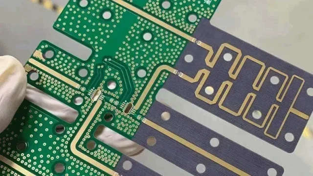
Manufacturing high-frequency signal PCBs requires strict process control to ensure electrical performance. Key factors include:
-
Precision impedance control during fabrication
-
Copper surface roughness management
-
Accurate dielectric thickness control
-
High-quality plating and lamination processes
Close collaboration between PCB designers and manufacturers ensures the final board meets performance requirements.
Conclusion
A well-designed High Frequency Signal PCB is essential for modern RF and high-speed communication systems. By selecting low-loss materials, optimizing PCB stackups, and implementing controlled impedance routing, engineers can ensure reliable signal transmission in GHz-frequency environments.
As wireless technologies and high-speed data systems continue to evolve, high-frequency PCB design will remain a critical component of advanced electronic engineering.
