
With the rapid development of technologies such as 5G communication, radar systems, satellite communication, automotive electronics, and high-speed computing, electronic systems are operating at increasingly higher frequencies.
Traditional PCB design methods are often insufficient for high-frequency applications because even small variations in:
- Trace geometry
- Material properties
- Layer structure
- Grounding design
- Manufacturing tolerance
can significantly affect signal performance.
High-frequency PCB design requires a combination of electrical simulation, material selection, controlled manufacturing processes, and advanced routing techniques to ensure:
- Low signal loss
- Stable impedance
- Reduced electromagnetic interference (EMI)
- Reliable high-speed transmission
This article introduces the essential design rules engineers should understand when developing high-frequency PCB boards.
1. Select Appropriate High-Frequency PCB Materials
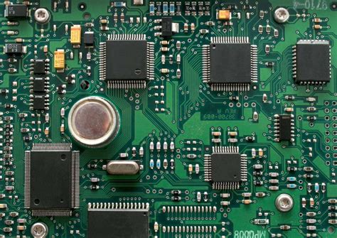
Material selection is one of the most critical factors in high-frequency PCB design.
Unlike standard FR-4 materials, high-frequency circuits often require specialized laminates with stable electrical characteristics.
Common high-frequency materials include:
1.1 Key Material Parameters
Dielectric Constant (Dk)
The dielectric constant affects:
- Signal propagation speed
- Impedance calculation
- Trace dimensions
A stable Dk value helps maintain consistent electrical performance.
Dissipation Factor (Df)
The dissipation factor determines dielectric loss.
Lower Df materials provide:
- Reduced insertion loss
- Better signal integrity
- Improved efficiency
This is especially important for:
- Microwave circuits
- RF communication systems
- Radar applications
Thermal Expansion Characteristics
High-frequency PCB materials should have stable thermal properties.
Important considerations include:
- Z-axis expansion
- Temperature variation
- Mechanical reliability
Poor thermal stability may cause:
- Layer deformation
- Via reliability problems
2. Design Controlled Impedance Routing
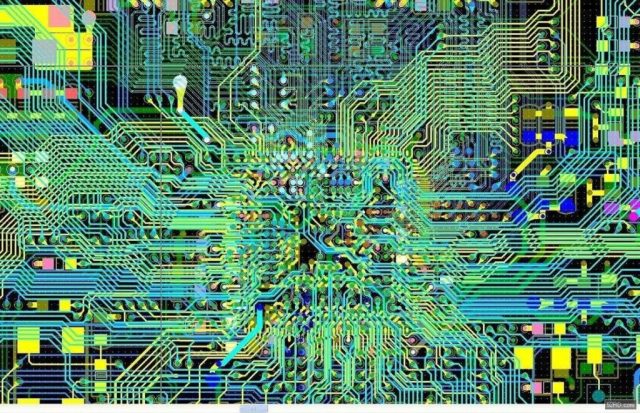
Impedance control is a fundamental requirement for high-frequency PCB design.
When signals operate at high frequencies, transmission lines behave differently from ordinary conductive traces.
Poor impedance matching may result in:
- Signal reflection
- Transmission loss
- Data distortion
2.1 Common Impedance Requirements
Typical high-frequency PCB designs use:
- 50Ω single-ended impedance
- 90Ω differential impedance
- 100Ω differential impedance
The required impedance depends on:
- Interface standards
- Application frequency
- System architecture
2.2 Factors Affecting Impedance
PCB impedance is influenced by:
- Trace width
- Copper thickness
- Dielectric thickness
- Dielectric constant
- Reference plane distance
Therefore, impedance control requires cooperation between:
- PCB designers
- Material suppliers
- PCB manufacturers
2.3 Impedance Verification
Manufacturers typically use:
- TDR (Time Domain Reflectometry)
to verify:
- Actual impedance value
- Manufacturing consistency
- Signal transmission performance
3. Optimize PCB Stack-Up Design
A proper stack-up structure is essential for high-frequency performance.
A high-frequency PCB stack-up usually includes:
- Signal layers
- Ground reference planes
- Power planes
- Dielectric layers
3.1 Maintain Signal Reference Planes
High-frequency signals require a stable return current path.
Recommended practices:
- Place high-speed signals near continuous ground planes
- Avoid unnecessary layer transitions
- Reduce return path discontinuities
Poor reference plane design may increase:
- EMI radiation
- Crosstalk
- Signal distortion
3.2 Symmetrical Stack-Up Design
A balanced stack-up helps reduce:
- PCB warpage
- Mechanical stress
- Manufacturing issues
Important factors include:
- Copper balance
- Dielectric thickness
- Material distribution
4. Minimize Signal Loss
Signal loss becomes more significant as frequency increases.
Main sources include:
- Dielectric loss
- Copper loss
- Surface roughness effects
4.1 Reduce Copper Surface Roughness
At high frequencies, current tends to flow near the conductor surface, known as the skin effect.
Excessive copper roughness increases:
- Insertion loss
- Transmission attenuation
Low-profile copper is often preferred for:
- RF circuits
- Microwave applications
- High-speed digital designs
4.2 Optimize Trace Length
High-frequency designs should minimize unnecessary routing length.
Benefits:
- Reduced propagation delay
- Lower signal attenuation
- Improved phase consistency
5. Follow Proper High-Frequency Routing Rules
5.1 Avoid Sharp Trace Corners
Sharp corners create impedance discontinuities.
Recommended:
- 45-degree routing
- Curved traces for RF circuits
Benefits:
- Smoother current flow
- Reduced reflection
5.2 Maintain Proper Trace Spacing
Insufficient spacing may increase:
- Crosstalk
- Electromagnetic coupling
Spacing should consider:
- Signal frequency
- Trace width
- Layer structure
5.3 Minimize Via Transitions
Vias introduce:
- Parasitic capacitance
- Inductance
- Impedance discontinuity
Design recommendations:
- Reduce unnecessary vias
- Use optimized via structures
- Consider back drilling for high-speed applications
6. Improve Grounding Design
Grounding is one of the most important aspects of high-frequency PCB design.
Poor grounding can cause:
- Increased noise
- EMI problems
- Signal instability
6.1 Use Continuous Ground Planes
A continuous ground plane provides:
- Stable return paths
- Reduced loop area
- Better shielding performance
6.2 Avoid Splitting High-Frequency Return Paths
High-frequency signals should not cross:
- Ground plane gaps
- Power plane interruptions
because return currents may be forced into longer paths.
6.3 Apply Ground Via Stitching
Ground vias can help:
- Reduce EMI radiation
- Improve grounding continuity
- Enhance shielding
Applications include:
- RF modules
- Microwave circuits
- Antenna boards
7. Consider Thermal Management
High-frequency circuits may generate significant heat, especially in:
- Power amplifiers
- RF transmitters
- Communication modules
Thermal design methods include:
- Thermal vias
- Copper areas
- Heat spreaders
- Metal core structures
Poor thermal management may affect:
- Frequency stability
- Component lifetime
- System reliability
8. Pay Attention to EMI and Shielding Design
High-frequency signals are more sensitive to electromagnetic interference.
Design methods include:
Ground Shielding
Use:
- Ground planes
- Shielding layers
- Via fences
Signal Isolation
Separate:
- High-frequency circuits
- Digital switching circuits
- Power circuits
This reduces unwanted coupling.
Controlled Routing Areas
Sensitive RF paths should avoid:
- Noisy power sections
- High-current traces
- Fast-switching signals
9. Manufacturing Considerations for High-Frequency PCBs
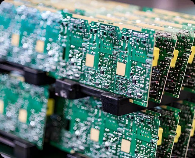
High-frequency PCB performance depends not only on design but also manufacturing accuracy.
Important manufacturing controls include:
Material Handling
Special materials require:
- Proper storage
- Controlled processing conditions
Precise Etching Control
Trace width variation directly affects:
- Impedance accuracy
- Signal performance
Layer Registration
High-frequency multilayer boards require:
- Accurate alignment
- Stable lamination processes
Surface Finish Selection
Common options:
ENIG
Suitable for:
- Fine-pitch components
- General high-frequency applications
ENEPIG
Suitable for:
- High-reliability applications
- Advanced packaging
10. Testing Requirements for High-Frequency PCBs
High-frequency PCB testing should include:
Impedance Testing
Used to verify:
- Trace impedance
- Manufacturing consistency
Network Analysis
Vector Network Analyzer (VNA) testing evaluates:
- Insertion loss
- Return loss
- Frequency response
Signal Integrity Analysis
Used to evaluate:
- Reflection
- Crosstalk
- Transmission quality
11. Common High-Frequency PCB Design Mistakes
Using Standard Materials Without Evaluation
Incorrect material selection may cause:
- Excessive signal loss
- Unstable performance
Ignoring Manufacturing Capability
A design may fail if it exceeds:
- Line width capability
- Registration tolerance
- Material processing limits
Poor Grounding Strategy
Problems include:
- EMI radiation
- Noise coupling
- Signal degradation
Excessive Via Usage
Too many vias may introduce:
- Signal discontinuity
- Additional parasitic effects
12. Applications of High-Frequency PCB Technology
RF Communication Systems
Applications:
- 5G base stations
- Wireless modules
- Satellite communication
Requirements:
- Low loss
- Stable impedance
Automotive Radar Systems
Applications:
- 24GHz radar
- 77GHz radar sensors
Requirements:
- Phase stability
- High-frequency reliability
Aerospace Electronics
Applications:
- Navigation systems
- Satellite equipment
Requirements:
- Environmental stability
- High reliability
Medical Electronics
Applications:
- Imaging equipment
- Monitoring systems
Requirements:
- Signal accuracy
- Low interference
Conclusion
High-frequency PCB design requires a comprehensive approach combining:
- Proper material selection
- Controlled impedance design
- Optimized stack-up structure
- Effective grounding
- EMI control
- Manufacturing precision
Unlike conventional PCB design, high-frequency circuits are highly sensitive to small design and manufacturing variations. Engineers must consider electrical performance from the earliest design stage and work closely with PCB manufacturers to ensure reliability.
By following proper high-frequency PCB design rules, electronic systems can achieve better signal integrity, lower transmission loss, and stable performance in demanding applications such as RF communication, radar, aerospace, and high-speed electronics.
