What Is a High Density PCB?
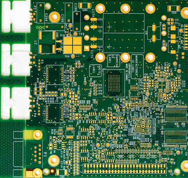
A High Density PCB (High Density Printed Circuit Board) is designed to accommodate more components, higher pin counts, and finer routing within a limited board area. It is widely used in applications that require compact size, high performance, and complex signal routing, such as semiconductor testing, telecommunications, automotive electronics, and advanced industrial systems.
High density PCBs typically incorporate HDI technology, microvias, fine line/space designs, and multilayer stackups.
Why High Density PCBs Are Essential
As electronic devices continue to shrink while performance requirements increase, traditional PCB designs are no longer sufficient. High density PCBs solve challenges such as:
-
Limited board space with increasing functionality
-
High pin count ICs and fine-pitch packages
-
High-speed and mixed-signal routing
-
Signal integrity and power integrity control
-
Thermal management in compact designs
High density PCBs enable reliable performance without increasing board size.
Key Features of High Density PCBs
A high-quality high density PCB typically includes:
-
Fine line and space routing
-
Microvias, blind vias, and buried vias
-
High layer count structures
-
Controlled impedance traces
-
Optimized ground and power planes
These features ensure stable electrical performance in dense layouts.
High Density PCB Design Considerations
Designing high density PCBs requires advanced engineering expertise, including:
-
Signal integrity analysis for high-speed nets
-
Proper via-in-pad and microvia structures
-
Layer stackup optimization
-
Crosstalk and EMI control
-
Thermal relief and heat dissipation planning
Well-executed design directly improves reliability and manufacturability.
Materials Used in High Density PCBs
Material selection is critical for high density PCBs performance. Common materials include:
-
High-Tg FR-4 for general high-density designs
-
Low-loss laminates for high-speed and RF applications
-
Hybrid material stackups for mixed-signal boards
-
High-reliability materials for harsh environments
Choosing the right material ensures consistent electrical and mechanical performance.
Manufacturing Capabilities for High Density PCBs
Producing high density PCBs requires advanced fabrication capabilities such as:
-
HDI PCB manufacturing
-
Laser-drilled microvias
-
Tight registration control
-
Advanced lamination processes
-
AOI and electrical testing
Strict process control guarantees yield and long-term reliability.
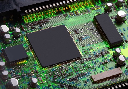
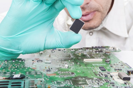
Assembly Challenges in High Density PCBs
High density PCB assembly often involves:
-
Fine-pitch BGA and CSP components
-
High pin count ICs
-
Precise solder paste printing
-
Advanced reflow profiles
-
X-ray inspection for hidden joints
Professional assembly ensures stable electrical connections in dense layouts.
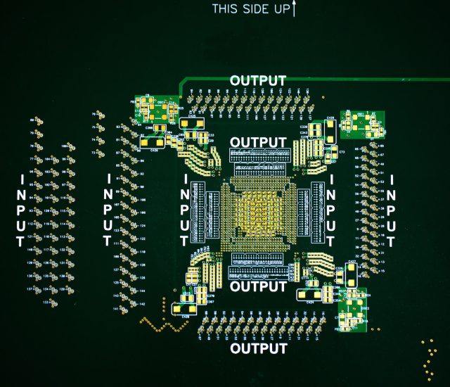
Applications of High Density PCBs
High density PCBs are widely used in:
-
Semiconductor test boards and ATE systems
-
IC test PCBs and load boards
-
5G and high-speed communication equipment
-
Automotive electronics and ADAS systems
-
Industrial automation and robotics
-
Medical and wearable devices
They are essential for modern compact electronic systems.
Why Choose a Professional High Density PCB Manufacturer
An experienced high density PCB manufacturer provides:
-
Strong HDI engineering support
-
Stable quality for complex designs
-
Fast turnaround for prototypes
-
Small-batch and volume production
-
One-stop PCB fabrication and assembly services
The right partner helps reduce risk and accelerate product development.
