A High Density PCB (HDPCB) is a multilayer, fine-pitch printed circuit board designed to support compact electronic devices, high-speed digital systems, and high-frequency applications. HDPCBs are widely used in telecommunications, 5G, IoT, automotive electronics, and high-performance computing, where space constraints, high pin counts, and advanced signal integrity requirements demand precise PCB engineering.
High density PCB design allows engineers to fit more functionality into smaller footprints without compromising electrical performance. Advanced HDI (High-Density Interconnect) structures, microvias, and multilayer stackups make it possible to achieve fine routing, controlled impedance, and minimal crosstalk in dense electronic systems.
Key Features and Benefits of High Density PCBs
1. Fine-Pitch and High Pin Count Support
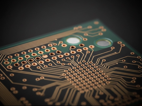
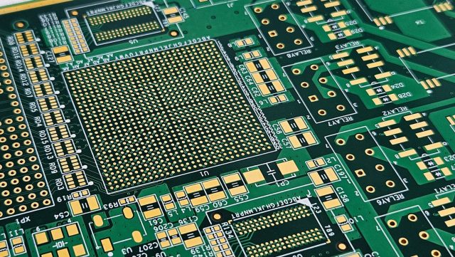
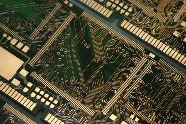
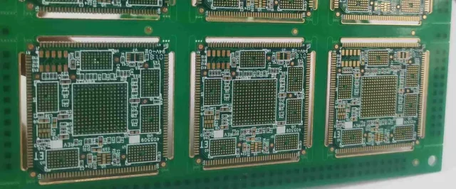
HDPCBs enable fine-pitch component placement, supporting ICs with high I/O counts. Microvias and blind/buried via technology allow compact fan-out without sacrificing signal quality.
2. Multilayer HDI Structure
Multiple layers provide dense routing channels for complex circuits, separating power, ground, and signal layers while maintaining signal integrity.
3. Controlled Impedance and Signal Integrity
High-speed digital and RF circuits require precise controlled impedance. Proper stackup design reduces signal reflection, insertion loss, and timing errors.
4. Power and Ground Optimization
Optimized power and ground planes ensure low impedance paths for stable power delivery and minimize voltage drops, noise, and crosstalk in high-density designs.
5. Compact Design with Reliability
By using HDI techniques, high density PCBs reduce overall board size, enhance mechanical stability, and maintain long-term reliability in harsh operating conditions.
Applications of High Density PCBs
High density PCBs are essential in:
-
5G and RF communication devices
-
IoT and wearable electronics
-
Automotive and ADAS systems
-
High-speed computing and servers
-
Aerospace and defense electronics
These applications require high pin density, high reliability, and precise signal integrity, making HDPCBs the preferred choice for modern electronics.
Manufacturing Capabilities for High Density PCBs
Producing HDPCBs requires advanced capabilities, including:
-
HDI multilayer PCB fabrication with microvias and blind/buried vias
-
Controlled impedance verification and testing
-
High-precision drilling and fine-line etching
-
Prototype, small batch, and mass production support
-
High-Tg and low-loss laminates for high-speed applications
Advanced manufacturing ensures consistent performance, reduced defects, and reliable high-speed operation.
Conclusion
A High Density PCB is a cornerstone for modern compact and high-performance electronics, enabling fine-pitch ICs, high-speed signal transmission, and reliable operation in space-constrained designs. By leveraging HDI technology, multilayer structures, controlled impedance, and optimized power distribution, high density PCBs provide engineers with the tools to meet the demands of 5G, IoT, automotive, and high-speed computing applications.
Partnering with an experienced high density PCB manufacturer ensures design accuracy, electrical reliability, and consistent production quality, supporting innovative electronics development.
