As electronic devices become smaller, faster, and more complex, traditional PCB technologies often reach their physical limits. HDI PCB (High Density Interconnect PCB) technology was developed to overcome these challenges by enabling higher wiring density, finer geometries, and improved electrical performance.
A professionally manufactured HDI PCB is a key enabler for modern consumer electronics, communication systems, and semiconductor test hardware.
What Is an HDI PCB?
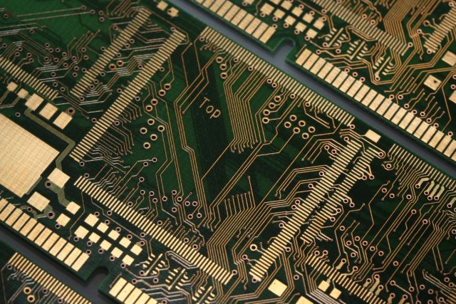
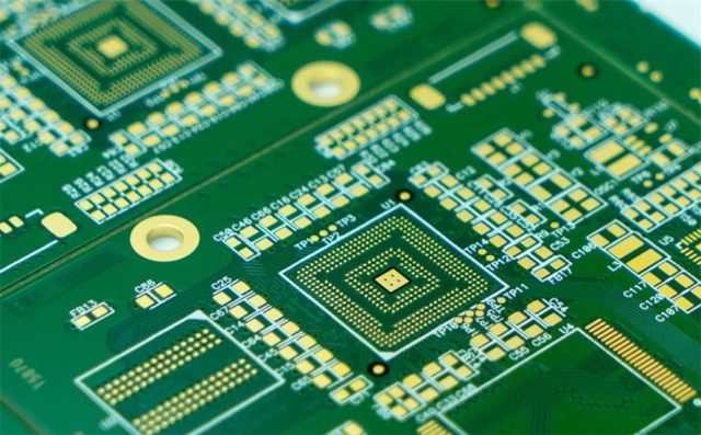
An HDI PCB is a printed circuit board that uses advanced interconnection techniques such as microvias, fine lines, and high-layer-count stackups to achieve significantly higher routing density than conventional PCBs.
HDI PCBs are characterized by:
-
Microvias (blind and buried vias)
-
Fine line and space routing
-
Thin dielectric layers
-
Sequential lamination processes
These features allow more connections to be routed in limited board space.
Why HDI PCB Technology Matters
HDI PCB technology delivers several critical advantages:
-
Smaller board size and thinner profiles
-
Improved signal integrity for high-speed designs
-
Better power distribution efficiency
-
Support for high pin count components
As device complexity increases, HDI PCBs become essential rather than optional.
Microvia Technology in HDI PCBs
Microvias are the foundation of HDI PCB design. Compared to traditional through-holes, microvias:
-
Occupy less routing space
-
Reduce parasitic inductance and capacitance
-
Enable shorter signal paths
Stacked and staggered microvia structures allow efficient breakout from dense BGA packages.
Signal Integrity Benefits of HDI PCBs
High-speed signals benefit significantly from HDI technology. HDI PCBs help improve signal integrity by:
-
Shortening interconnect lengths
-
Reducing impedance discontinuities
-
Minimizing crosstalk and reflections
These benefits are especially important for high-speed digital and RF applications.
Power Integrity and Layer Stackup Optimization
HDI PCBs support advanced power distribution strategies:
-
Thin dielectric layers reduce loop inductance
-
Closely coupled power and ground planes
-
Improved decoupling capacitor placement
This results in cleaner power delivery and more stable system operation.
Materials Used in HDI PCBs
Material selection plays a key role in HDI PCB performance:
-
High-Tg FR-4 for structural stability
-
Low-loss laminates for high-speed signals
-
Hybrid stackups for mixed-frequency designs
Proper material selection ensures electrical stability and manufacturability.
Manufacturing Challenges of HDI PCBs
Producing a reliable HDI PCB requires advanced manufacturing capabilities:
-
Laser drilling for microvias
-
Precise registration across multiple lamination cycles
-
Tight control of line width, spacing, and copper thickness
Experience and process control are essential for consistent quality.
Typical Applications of HDI PCBs
HDI PCBs are widely used in:
-
Smartphones and wearable electronics
-
High-speed communication equipment
-
Semiconductor test hardware
-
Automotive electronics and ADAS systems
These applications demand compact size and high performance.
HDI PCB vs Conventional PCB
Compared to conventional PCBs, HDI PCBs offer:
-
Higher routing density
-
Better electrical performance
-
Reduced board size
However, they require more advanced design and manufacturing expertise.
Choosing an HDI PCB Manufacturing Partner
When selecting an HDI PCB manufacturer, key considerations include:
-
Experience with microvia and sequential lamination
-
Capability for fine line and tight tolerance production
-
Strong quality control and inspection systems
-
Engineering support for complex designs
A skilled partner ensures successful HDI PCB implementation.
Conclusion
The HDI PCB represents a critical advancement in PCB technology, enabling compact, high-performance electronic systems through advanced interconnect techniques. By combining microvia technology, optimized stackups, and precise manufacturing processes, HDI PCBs support the next generation of electronic innovation.
Working with an experienced HDI PCB supplier is essential to achieve reliable performance from prototype to mass production.
