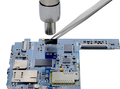
What Is Fine Pitch PCB?
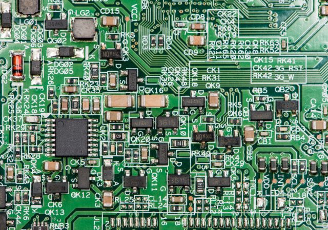
A Fine Pitch PCB refers to a printed circuit board designed with extremely small trace width and spacing to support high pin count and fine pitch components. It is commonly used in advanced electronic systems where compact design, high integration, and precise routing are essential.
Fine pitch designs are typically required for:
-
BGA and micro BGA packages
-
QFN and LGA packages
-
WLCSP components
-
High-speed processors
-
RF modules
-
Semiconductor test boards
As electronic components continue to shrink in size while increasing in performance, Fine Pitch PCB technology becomes increasingly important.
Key Features of Fine Pitch PCB
1. Ultra-Fine Line Width and Spacing
Fine Pitch PCB fabrication may support:
-
3/3 mil or smaller trace/space
-
Advanced etching processes
-
High-resolution imaging technology
Precise line control ensures signal stability and accurate connectivity for high-density layouts.
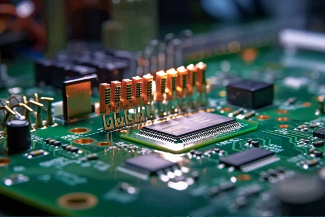
2. Support for High Pin Count Components
Fine pitch routing allows efficient breakout of:
-
High pin count BGA
-
Fine pitch IC packages
-
High-speed digital processors
-
RF transceiver chips
This ensures reliable electrical performance even in compact layouts.
3. Advanced Via Structures
Fine Pitch PCB often integrates:
-
Microvias
-
Blind vias
-
Buried vias
-
Via-in-pad structures
These technologies improve routing flexibility and enable high-density interconnections.
4. High Signal Integrity Performance
With tighter routing and optimized stack-up design, Fine Pitch PCB supports:
-
Controlled impedance
-
Differential pair routing
-
Reduced crosstalk
-
Shorter signal paths
-
Improved high-frequency performance
This is critical for high-speed digital and RF applications.
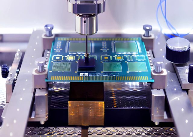
Manufacturing Capabilities
Professional Fine Pitch PCB fabrication may include:
-
HDI stack-up design
-
Sequential lamination
-
Laser drilling for microvias
-
Tight tolerance registration
-
Controlled impedance processing
-
High TG or low loss materials
-
Surface finishes such as ENIG or ENEPIG
Strict process control ensures dimensional accuracy and electrical stability.
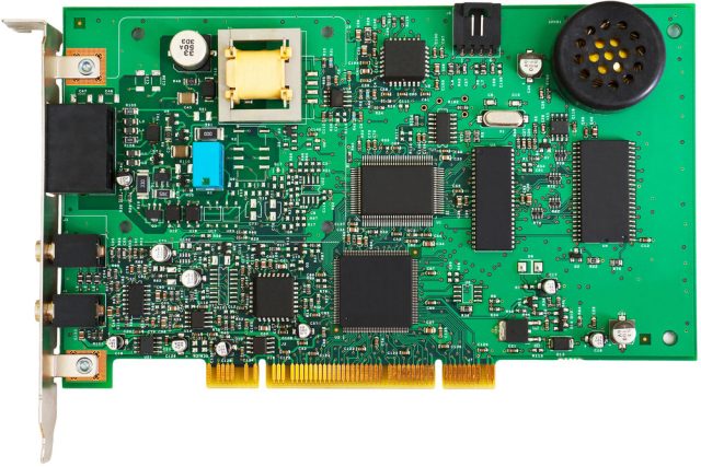
Applications of Fine Pitch PCB
Fine Pitch PCB is widely used in:
-
5G communication equipment
-
Semiconductor testing systems
-
High-speed computing boards
-
IoT devices
-
Automotive electronics
-
Medical electronics
-
Industrial automation systems
It plays a key role in enabling miniaturization and high-performance electronic design.
Advantages of Fine Pitch PCB
-
Higher component density
-
Reduced PCB size
-
Improved routing efficiency
-
Enhanced electrical performance
-
Support for advanced semiconductor packaging
-
Greater design flexibility
Fine Pitch PCB is essential for modern compact and high-speed electronics.
Conclusion
Fine Pitch PCB enables high-density routing and precise connectivity for advanced electronic systems. With ultra-fine line capability, microvia integration, and strict impedance control, it supports high-speed, RF, and semiconductor applications requiring precision and reliability.
Choosing an experienced PCB manufacturer ensures stable quality, tight tolerance control, and consistent performance for demanding fine pitch designs.
