A Fine Pitch PCB is a printed circuit board specifically designed to support high pin count ICs and ultra-small component spacing, commonly found in modern semiconductor devices, high-speed electronics, IoT modules, automotive electronics, and advanced test boards. As electronic products continue to shrink while integrating more functions, fine pitch PCB technology has become essential for achieving compact layouts, reliable soldering, and high signal integrity.
Fine pitch PCBs typically feature narrow trace widths, tight spacing tolerances, advanced multilayer stackups, and microvia structures, enabling engineers to route dense interconnections without compromising electrical performance.
Key Characteristics of Fine Pitch PCBs
1. Ultra-Fine Line Width and Spacing
Fine pitch PCBs use fine-line routing, often at very tight trace width and spacing, to accommodate ICs with small pad pitches. This allows high-density routing while maintaining electrical reliability.
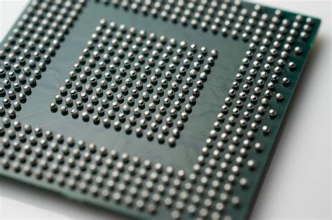
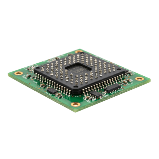
2. High Pin Count IC Support
Modern fine pitch designs support high pin count packages, enabling stable connections for complex ICs used in processors, memory devices, and high-speed communication chips.
3. Microvia and Via-in-Pad Technology
To maximize routing density, fine pitch PCBs commonly integrate microvias, blind and buried vias, and via-in-pad designs, which reduce parasitic effects and save valuable board space.
4. Advanced Multilayer Stackups
Fine pitch PCBs often rely on multilayer constructions to separate signal, power, and ground layers, improving signal integrity, noise control, and EMI performance.
5. Controlled Impedance Routing
For high-speed and RF applications, fine pitch PCBs incorporate controlled impedance traces and differential pair routing, ensuring stable signal transmission even in dense layouts.
Advantages of Fine Pitch PCBs
-
Supports compact and miniaturized product designs
-
Enables high routing density for complex ICs
-
Improves signal integrity and electrical performance
-
Enhances soldering reliability for fine-pitch components
-
Reduces PCB size without sacrificing functionality
Applications of Fine Pitch PCBs
Fine pitch PCBs are widely used in:
-
Semiconductor test boards and IC test PCBs
-
High-speed digital and RF communication systems
-
IoT devices and wearable electronics
-
Automotive electronics and ADAS modules
-
Consumer electronics with compact form factors
In each application, fine pitch PCB technology ensures reliable interconnections and stable electrical performance.
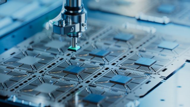
Manufacturing Requirements for Fine Pitch PCBs
Producing high-quality fine pitch PCBs requires:
-
Tight control of trace width, spacing, and alignment
-
Advanced imaging and etching processes
-
Precision drilling and microvia fabrication
-
Accurate solder mask registration
-
Electrical testing and quality inspection
An experienced manufacturer ensures high yield, consistent quality, and reliable assembly performance for fine pitch PCB projects.
Conclusion
A Fine Pitch PCB is essential for modern electronics that demand high pin count connectivity, compact layouts, and high electrical performance. By combining fine-line routing, advanced multilayer stackups, microvia technology, and controlled impedance design, fine pitch PCBs deliver reliable signal integrity and manufacturing precision.
Choosing a professional fine pitch PCB manufacturer ensures consistent quality, reliable performance, and efficient support from prototyping through mass production.
