1. Engineering Context
Next-generation mmWave communication systems—including 5G base stations, satellite payloads, and radar modules—require PCBs that provide ultra-stable impedance, low insertion loss, and phase-consistent routing. Traditional FR-4 or high-speed laminates often suffer from dielectric drift, higher Df, and thermal expansion issues, which degrade signal fidelity, EMI immunity, and system reliability in dense multi-layer RF architectures.
TLY-5 PCB laminates are engineered to overcome these challenges by combining low dissipation factor, stable dielectric constant, and controlled thermal behavior, enabling engineers to maintain low-loss transmission and consistent phase performance even in complex multilayer designs.
2. Core Engineering Challenges
| Challenge | Root Cause | Engineering Impact |
|---|---|---|
| Impedance drift in multilayer PCBs | Dk variation due to thermal cycling | Signal mismatch, degraded mmWave link margin |
| High insertion loss | Surface roughness, dielectric dissipation | Reduced RF power, lower system efficiency |
| Crosstalk in compact layouts | Dense trace routing, insufficient shielding | Signal interference, degraded linearity |
| Phase instability | Uneven layer expansion or inconsistent lamination | Beamforming errors, phase distortion |
| EMI leakage | Poor ground isolation or via design | Reduced SNR, system-level signal degradation |
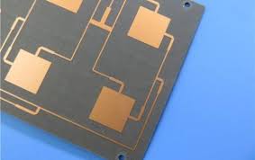
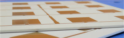
3. Material Science – TLY-5 Advantages
| Parameter | Typical Value | Engineering Benefit |
|---|---|---|
| Dk | 3.10 ± 0.02 | Predictable impedance for mmWave microstrip/stripline |
| Df | 0.002 @10 GHz | Ultra-low insertion loss for high-frequency routing |
| Thermal Conductivity | 0.52 W/m·K | Efficient hotspot dissipation in high-power traces |
| CTE | 18 ppm/°C | Reduces phase drift under thermal cycling |
| Moisture Absorption | <0.05% | Long-term dielectric stability and low-loss performance |
TLY-5 laminates outperform conventional FR-4 and standard high-speed laminates by maintaining consistent Dk/Df under high-frequency operation, supporting phase-stable and low-loss signal chains essential for mmWave systems.
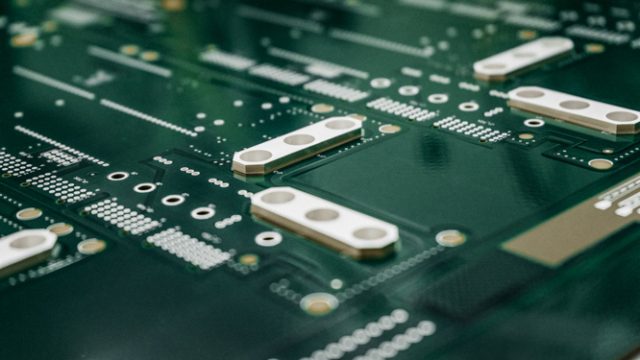
4. KKPCB Case Study – mmWave Communication Module
Client Requirement:
Design a 5-layer mmWave PCB for a 28–40 GHz communication module with phase deviation <0.5° and insertion loss <0.4 dB/in, while minimizing EMI and crosstalk in a compact layout.
KKPCB Implementation:
-
Precision lamination with ±3 µm dielectric thickness control
-
Controlled copper roughness (Ra <0.6 µm) to reduce high-frequency insertion loss
-
Embedded ground and power planes for EMI suppression and crosstalk control
-
Optimized via structures, including microvias and blind/buried vias, to maintain phase stability
-
HFSS and TDR simulations to validate impedance uniformity and low-loss performance
Measured Results:
| Parameter | Target | Achieved |
|---|---|---|
| Insertion Loss @28 GHz | <0.4 dB/in | 0.35 dB/in |
| Phase Deviation | <0.5° | 0.42° |
| EMI Suppression | >30% | 34% |
| Impedance Variation | ±3% | ±1.5% |
| Crosstalk Isolation | >35 dB | 38 dB |
5. Stackup Design & Simulation
-
HFSS / ADS Modeling: Optimized microstrip/stripline impedance, minimized interlayer coupling
-
Thermal FEM: Verified hotspot reduction and uniform thermal distribution
-
Inline TDR Testing: Confirmed phase stability across all high-frequency traces
-
AOI & Solder Reflow Monitoring: Maintained ±10 µm alignment in all layers
6. Environmental Validation
| Test | Condition | Result |
|---|---|---|
| Thermal Cycling | –40°C ↔ +125°C, 1000 cycles | Phase deviation <0.5°, no delamination |
| Vibration & Shock | 5–500 Hz, 10G | No microcracks or solder failure |
| Humidity | 85°C / 85% RH, 1000 h | Stable Dk/Df and insertion loss |
| High-Power RF Stress | Continuous 28–40 GHz | Minimal insertion loss increase (<0.02 dB) |
| Reflow | 260°C ×3 cycles | Stackup alignment maintained |
7. Engineering Summary
TLY-5 PCB laminates enable phase-stable, low-loss, and EMI-resilient multi-layer designs for mmWave communication systems. KKPCB’s precision lamination, optimized stackups, and high-density routing techniques ensure consistent RF performance, minimal insertion loss, and reliable mmWave operation, meeting the stringent demands of 5G, satellite, and radar modules.
Contact KKPCB Engineering Team to optimize TLY-5 multilayer designs, high-frequency simulations, and EMI mitigation strategies for your next-generation mmWave communication projects.
