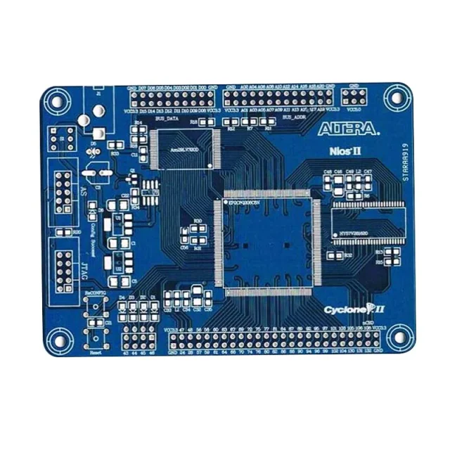
As RF communication, IoT edge devices, automotive radar, and compact wireless modules continue to evolve, the Double Layer HF PCB has become a preferred architecture for delivering high-frequency stability, low insertion loss, and predictable electromagnetic performance. Although limited to two copper layers, a Double Layer HF PCB—when engineered correctly—can outperform many multilayer structures in signal consistency, impedance integrity, and RF power efficiency.
This article explores how material science, stackup control, and precision manufacturing come together to form a high-performance Double Layer HF PCB suitable for modern RF and microwave applications.
1. High-Frequency Engineering Context
A Double Layer HF PCB is not simply a “2-layer RF board.” It is a highly engineered RF platform designed to achieve:
-
Low dielectric loss for GHz-level signals
-
Stable and repeatable impedance across production batches
-
Minimal conductor loss with low-profile copper
-
Clean ground reference for microstrip and coplanar structures
-
Thermal and frequency stability under varying environmental conditions
Where system footprint, cost, or antenna integration prevents multilayer construction, a Double Layer HF PCB provides exceptional RF performance-to-cost efficiency.
2. Material Science Driving High-Frequency Behavior
The performance of a Double Layer HF PCB is defined almost entirely by its dielectric substrate, making material selection the most critical engineering decision.
Key High-Frequency Properties
• Dielectric Constant (Dk) Stability
A precise and stable Dk enables consistent impedance, faster propagation velocity, and reduced phase distortion.
• Dissipation Factor (Df / Loss Tangent)
Lower Df directly translates into lower insertion loss—critical in WiFi, BLE, GPS, radar, and 5G sub-6 GHz RF chains.
• TCDk (Thermal Coefficient of Dielectric Constant)
Prevents impedance drift during temperature swings, essential for outdoor IoT and telecom devices.
• Copper Foil Type (RA, ED, Rolled)
Determines conductor loss under skin-effect dominance at high frequencies.
Preferred HF Materials at KKPCB
-
Rogers RO4350B / RO4003C
-
PTFE composites
-
Hydrocarbon-ceramic laminates
-
Low-roughness copper substrates
These materials allow a Double Layer HF PCB to achieve exceptional RF clarity even at frequencies approaching 10 GHz.
3. High-Frequency Stackup Strategy for Double Layer HF PCB
Although the structure is simple—Cu / HF Dielectric / Cu—the engineering considerations behind this stackup are not.
Critical Stackup Parameters
• Core Thickness Optimization
Defines microstrip impedance and affects phase delay. Deviations as small as ±10 µm can shift impedance by several ohms.
• Consistent Copper Thickness
Enables precise impedance tuning and stable propagation at high frequencies.
• Surface Roughness Control
Lower roughness = lower conductor loss, vital for microwave systems.
• Solder Mask Management
Many RF traces on Double Layer HF PCB are intentionally mask-free to reduce dielectric loading and improve consistency.
• Bottom-Layer Ground Integrity
An uninterrupted ground plane is the backbone of RF stability, reducing noise coupling and improving return-path behavior.
4. RF Routing & Electromagnetic Optimization
A Double Layer HF PCB relies heavily on microstrip or coplanar waveguide (CPWG) structures to maintain controlled impedance and electromagnetic isolation.
Engineering Best Practices
-
Maintain RF line width tolerance within ±0.02 mm
-
Use CPWG for tighter confinement and reduced EMI
-
Replace all 90° turns with mitred or arc bends
-
Avoid via transitions to reduce reflection and radiation
-
Use dense ground-via stitching around RF paths
-
Keep RF sections isolated from noisy digital power regions
With these design rules, a Double Layer HF PCB can deliver consistent high-frequency behavior even under tight form-factor constraints.
5. KKPCB Manufacturing Precision for Double Layer HF PCB
KKPCB leverages advanced HF PCB engineering capabilities to enhance performance:
-
High-frequency substrate lamination control
-
Ultra-tight dielectric thickness tolerance
-
Low-profile copper for reduced conductor loss
-
Laser direct imaging for RF trace accuracy
-
Precise impedance modeling and certification
-
RF testing (S-parameters, RL/IL, time-domain impedance)
These capabilities ensure that every Double Layer HF PCB manufactured at KKPCB delivers stable, repeatable, production-grade RF performance.
6. Engineering Summary
A Double Layer HF PCB remains one of the most efficient ways to realize high-frequency and microwave designs where stability, low loss, and compact construction are required. With the right combination of HF materials, precision stackup control, advanced routing practices, and tight manufacturing tolerances, a Double Layer HF PCB can outperform expectations—making it a critical building block in:
-
IoT RF modules
-
GNSS/GPS antennas
-
2.4 GHz / 5.8 GHz WiFi systems
-
BLE/Zigbee modules
-
Microwave sensors
-
Automotive radar subsystems
Through advanced HF engineering, KKPCB transforms Double Layer HF PCB into a reliable, low-loss, and production-ready RF platform for modern wireless technologies.
