
Contents
Duroid 6002 PCB projects are often selected for low-loss microwave behavior, then challenged by stackup substitutions, via transitions, and panel process changes. The project pain point is usually not the material name. It is the gap between the RF model, the pressed construction, and the evidence used to release production. This guide gives a practical engineering method without presenting unverified customer measurements.
Why low-loss stackup choices drift
A Duroid 6002 PCB is a finished laminate-and-copper construction. Pressed dielectric thickness, copper foil, roughness, drilled holes, plating, and reference-plane continuity all affect the field. A supplier datasheet provides typical material information, but the approved board still needs a controlled stackup and a manufacturable process window.
Freeze the Duroid 6002 PCB drawing, material lot, copper weights, and impedance targets together. A high-frequency PCB design review should distinguish typical material values, engineering targets, and measured coupon evidence.
Seven controls for a stable release
1. Approve finished dielectric targets
Record the finished dielectric thickness after lamination, not only the nominal core. Identify press construction, bondply, copper foil, and sequential steps. Every Duroid 6002 PCB release should point to one stackup revision used by the field model.
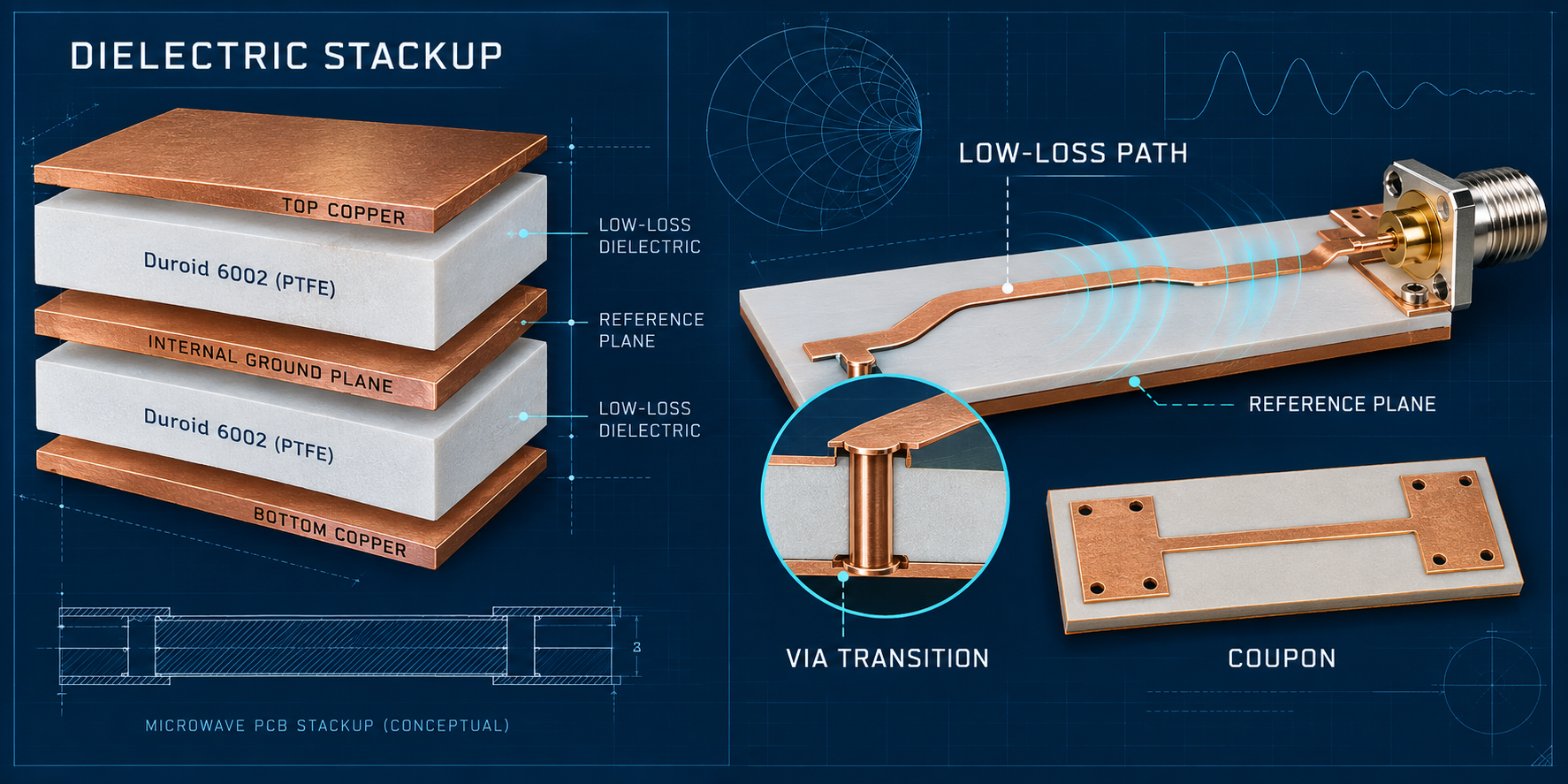
Conceptual low-loss stackup, reference plane, via transition, and coupon.
2. Tie trace geometry to the stackup
Keep trace width, copper thickness, reference-plane distance, and dielectric target visible on the RF drawing. If the fabricator proposes a different construction, reopen the field review. The PCB materials record should identify the manufacturer data used as the starting point.
3. Treat copper profile as a controlled variable
Copper roughness and foil profile influence loss and effective impedance. State the assumption on the stackup drawing and align etch compensation and plating with it. A PCB manufacturing review should link foil, etch, plating, and cross-section checks.
4. Plan transitions, not just straight traces
Review connector launches, vias, bends, and layer changes as part of the low-loss path. On a Duroid 6002 PCB, an unplanned reference-plane void can dominate the transition even when the straight trace is correct.
5. Define a representative coupon
Use coupon geometries that represent the critical microstrip, coplanar, via, or connector transition. Define coupon location, fixture, calibration, frequency range, and acceptance method before production. A coupon is process evidence for that revision, not a customer case study.
6. Align drilling and plating with RF intent
The Duroid 6002 PCB process record should tie via geometry to drilling, plating, and registration evidence.
Finished hole, annular ring, plating, and registration limits must fit the via and connector design. For a multilayer PCB build, identify sequential-lamination and back-drill features on the same release drawing.
7. Carry the stackup into assembly
A Duroid 6002 PCB assembly handoff should retain the approved stackup and connector datum.
Connector seating, solder fillets, fixtures, and cleaning can move an RF launch. A PCB assembly traveler should reference the same datums and revision as the Duroid 6002 PCB fabrication package.
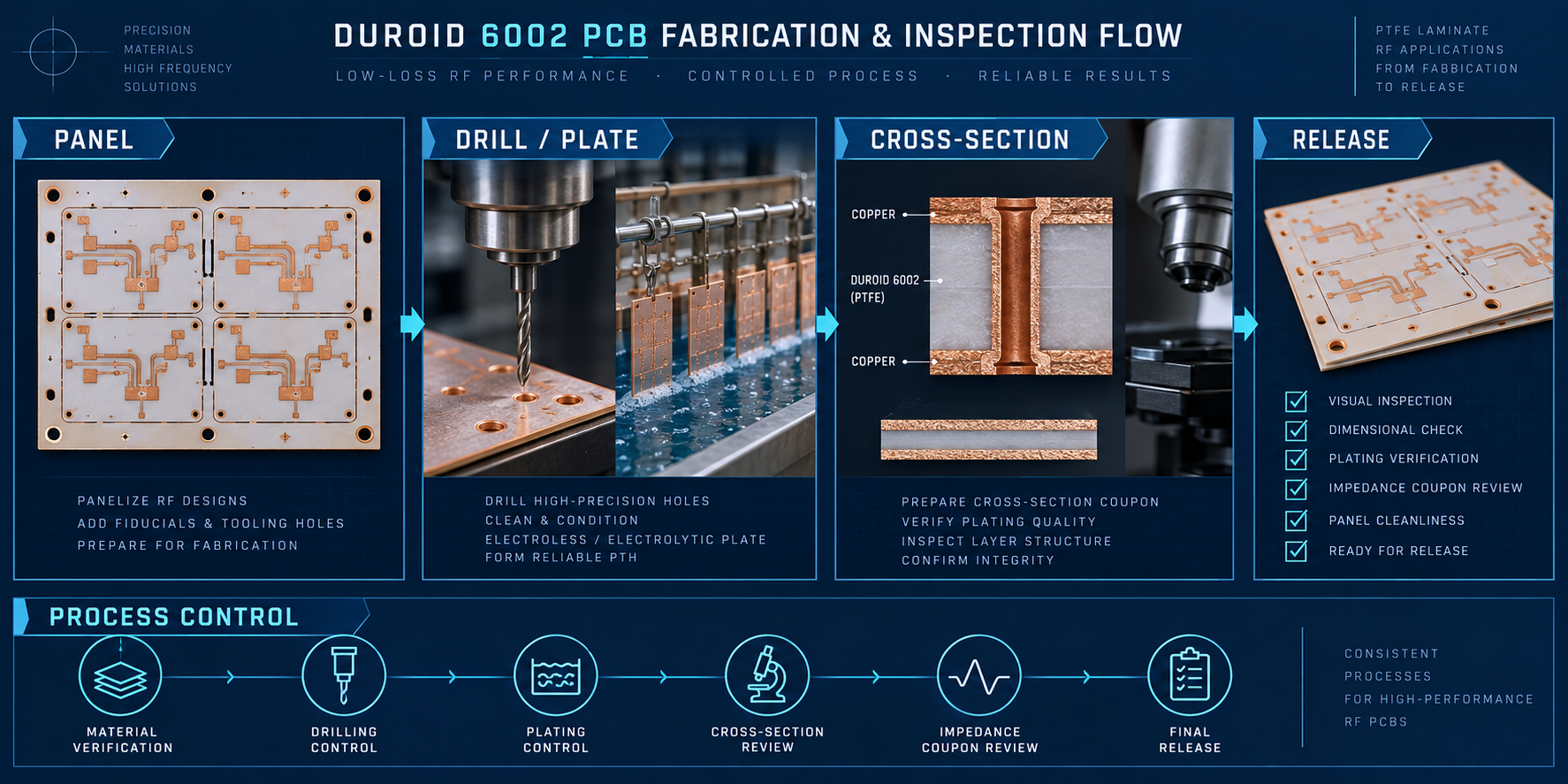
Conceptual panel, drill/plating, cross-section, and release flow.
Fabrication and inspection flow
Move from MATERIAL VERIFICATION to PANEL to DRILL/PLATE to CROSS-SECTION to COUPON REVIEW and RELEASE. Retain the material certificate, panel map, process revision, coupon location, and inspection disposition. If the press cycle or copper foil changes, repeat the review before the next Duroid 6002 PCB lot.
Duroid 6002 PCB project checklist
- Finished dielectric, copper, and press targets are revision controlled.
- Field-model assumptions match the approved stackup and transitions.
- Typical, target, and measured values are labeled separately.
- Coupon geometry represents the critical RF path.
- Drill, plating, registration, and panel limits are manufacturable.
- Assembly fixtures and connector datums match the RF drawing.
The approved Duroid 6002 PCB package should remain the single source for design, fabrication, coupon, and assembly decisions. Add a second Duroid 6002 PCB reference only when it points to the same controlled material page, not an article page.
Sources: Rogers Corporation RT/duroid 6002 material information and fabrication guidance; IPC-TM-650 methods for dielectric, drilling, plating, registration, and impedance-related checks; KKPCB internal high-frequency DFM capability notes. Values are typical or target references unless explicitly identified as measured.
