
Contents
Duroid 6002 PCB designs for outdoor or high-duty microwave modules must hold RF geometry while the board moves through thermal conditioning, panel processing, and connector assembly. The practical project problem is registration drift between antenna features, reference planes, holes, and the launch datum. This guide provides a controlled review method and separates process targets from measured evidence.
Why thermal registration matters
A Duroid 6002 PCB combines low-loss laminate, copper, plated holes, and mechanical features. Temperature and humidity conditioning can expose differences between the RF artwork and the mechanical reference used in fabrication. A connector launch can remain visually acceptable while its signal pad and return vias no longer share the intended datum.
Freeze the Duroid 6002 PCB panel origin, fiducials, stackup, and connector drawing together. A high-frequency PCB design review should show X-Y registration, layer alignment, and the planned conditioning sequence.
Six controls for stable microwave geometry
1. Use one panel datum
Dimension array cells, drill locations, connector holes, and inspection targets from a master datum. Do not use a trimmed edge as the only reference. Every Duroid 6002 PCB panel should carry the same origin through imaging, drilling, routing, and assembly.
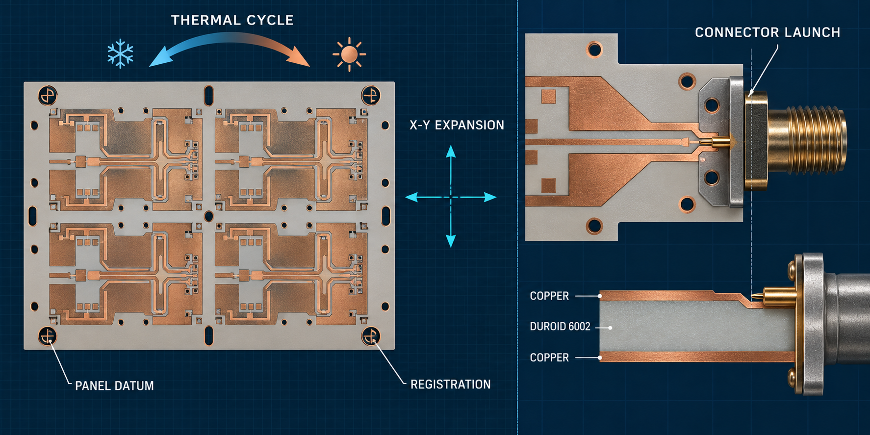
Conceptual thermal cycle, panel datum, X-Y expansion, and connector launch registration.
2. Define the stackup after press
Record finished dielectric thickness, copper foil, press construction, and sequential steps after lamination. Manufacturer typical values are inputs, not a substitute for the approved board stackup. Keep the PCB materials record linked to the same revision as the RF model.
3. Protect fiducials and tooling holes
A Duroid 6002 PCB manufacturing datum must remain readable after imaging and drilling.
Place global and local fiducials where copper, mask, and routing will not erase them. Tooling holes must fit the drill and panel process. A PCB manufacturing handoff should show the datum, compensation revision, and center-to-edge inspection plan.
4. Coordinate the connector launch
Connector holes, signal pad, ground pads, and first return vias should reference one mechanical axis. If the connector vendor changes, compare flange, pin, mounting, and insertion geometry before release. The PCB assembly traveler should identify seating and torque features that can move the launch.
5. Plan conditioning and recovery
Define the conditioning sequence, dwell points, recovery time, and inspection method before production. A coupon or witness panel can show whether a target remains readable after the agreed cycle. Keep target, typical, and measured labels separate.
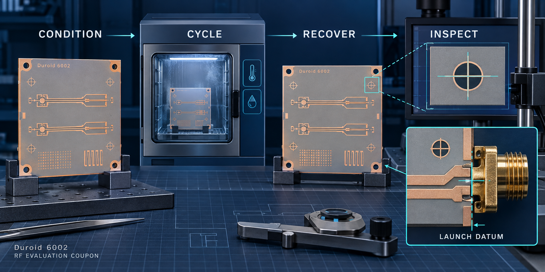
Conceptual condition, cycle, recover, inspect flow with launch datum.
6. Compare center and edge locations
For a Duroid 6002 PCB panel, retain center and edge evidence with the same revision.
Uneven copper density, routing, or panelization can create different registration conditions. Inspect representative center and edge locations, then retain the map with the multilayer PCB build record.
Conditioning and inspection flow
Move from CONDITION to CYCLE to RECOVER to INSPECT. Record the panel revision, material lot, fixture, measurement method, and disposition. This process evidence belongs to the specific Duroid 6002 PCB revision; it is not a customer case study.
Duroid 6002 PCB project checklist
- One datum is shared by layout, panel, drill, assembly, and inspection.
- Finished stackup and material revision are frozen before release.
- Fiducials, tooling holes, connector holes, and RF features remain readable.
- Conditioning, recovery, and inspection steps are documented.
- Center and edge evidence is retained when copper density changes.
- Targets, typical values, and measured values are clearly labeled.
The approved Duroid 6002 PCB package should remain synchronized across design, fabrication, conditioning, and assembly. Add a second Duroid 6002 PCB reference only to the controlled material page.
Sources: Rogers Corporation RT/duroid 6002 material information and fabrication guidance; IPC-TM-650 methods for dimensional, drilling, plating, registration, and environmental conditioning checks; KKPCB internal high-frequency DFM capability notes. Values are typical or target references unless explicitly identified as measured.
