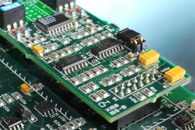
As electronic systems continue to evolve toward higher speed, smaller form factors, and increased functionality, traditional through-hole via structures are becoming a limiting factor. Buried Via PCB technology has emerged as a critical enabler for high-density routing and signal integrity optimization, particularly in HDI, high-speed digital, and RF applications.
By embedding vias between inner layers rather than extending them through the entire board thickness, buried via PCBs significantly improve routing efficiency while reducing electrical discontinuities. This article explores the engineering logic behind buried via PCB design and the key factors that impact signal integrity and manufacturability.
What Is a Buried Via PCB?
A buried via PCB is a multilayer printed circuit board in which vias connect only internal layers and do not appear on the outer surfaces. Unlike through vias, buried vias are formed and laminated during intermediate fabrication stages, making them invisible from the top and bottom layers.
This structure allows designers to reserve surface layers for fine-pitch component routing while maintaining robust interconnections within the internal stackup.
Why Buried Via PCBs Enable High-Density Routing
Maximizing Available Routing Channels
In high-density PCB layouts, surface real estate is extremely limited. Buried via PCBs remove unnecessary via pads and antipads from outer layers, freeing routing channels for:
-
High-speed differential pairs
-
Dense BGA fan-out
-
Power and ground distribution
This makes buried via PCB designs especially effective in HDI architectures where layer utilization efficiency directly affects board size and cost.
Reducing Via Congestion in Critical Areas
By strategically placing buried vias within specific layer pairs, designers can isolate dense routing zones and prevent via congestion near sensitive signal paths. This is essential for high-speed PCB and RF PCB designs, where electromagnetic coupling and impedance disturbances can degrade performance.
Signal Integrity Advantages of Buried Via PCB Design
Minimized Via Stub Effects
One of the most important signal integrity benefits of buried via PCBs is the reduction or elimination of via stubs. Via stubs act as resonant structures that introduce reflections, insertion loss, and phase distortion—especially at high frequencies.
Buried vias connect only the required layers, resulting in:
-
Lower reflection coefficients
-
Improved eye diagram performance
-
Better impedance continuity
This makes buried via PCB technology highly suitable for multi-gigabit digital interfaces and high-frequency signal paths.
Improved Impedance Control
Controlled impedance routing becomes more predictable in buried via PCB stackups. Since the via length and dielectric environment are tightly defined within internal layers, impedance variation caused by excess via length is minimized.
This enhances signal integrity in applications requiring strict impedance tolerances, such as:
-
High-speed serial links
-
RF transceivers
-
High-performance computing systems
Buried Via PCB Stackup Design Considerations
Layer Pair Planning
Effective buried via PCB design begins with careful layer pair planning. Designers must determine:
-
Which signal layers require buried interconnections
-
How power and ground planes are positioned
-
The lamination sequence needed to form buried vias
Poor layer planning can increase fabrication complexity or introduce unnecessary cost.
Balancing Electrical Performance and Manufacturability
While buried via PCBs offer significant electrical advantages, they also introduce additional lamination cycles and drilling steps. Engineering teams must balance:
-
Signal integrity requirements
-
Board thickness constraints
-
Yield and process capability
Early collaboration with the PCB manufacturer is essential to ensure that buried via PCB designs remain manufacturable at scale.
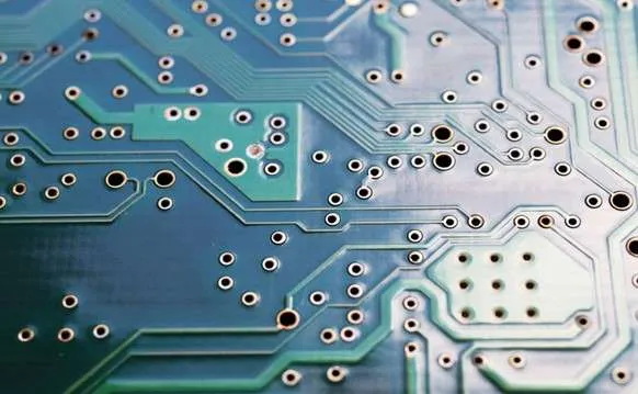
Manufacturing Challenges in Buried Via PCBs
Buried via PCB fabrication requires precise process control, including:
-
Sequential lamination accuracy
-
Via drilling and registration
-
Copper plating uniformity
-
Layer-to-layer alignment
At KKPCB, buried via PCB manufacturing is supported by advanced HDI process control and engineering review to ensure consistency between design intent and production reality.
Typical Applications of Buried Via PCB Technology
Buried via PCBs are widely used in applications where high routing density and signal integrity are equally critical, including:
-
HDI consumer electronics
-
High-speed networking equipment
-
RF and microwave modules
-
Industrial automation systems
-
Aerospace and defense electronics
In these systems, buried via PCB structures help achieve compact layouts without compromising electrical performance.
Conclusion
Designing buried via PCBs is no longer just an advanced option—it is a necessity for modern high-density and high-speed electronic systems. By enabling efficient routing, reducing via-related signal degradation, and supporting controlled impedance structures, buried via PCBs play a vital role in signal integrity optimization.
With deep experience in HDI stackups and sequential lamination processes, KKPCB provides engineering-driven buried via PCB solutions that balance performance, reliability, and manufacturability.
