What is a Ceramic PCB?
A Ceramic PCB is a printed circuit board built using ceramic substrates like alumina (Al₂O₃), aluminum nitride (AlN), or silicon nitride (Si₃N₄) instead of standard FR-4 or PTFE materials. These substrates are thermally conductive, electrically insulating, and mechanically robust, making them ideal for high-power electronics and RF/microwave applications.
Ceramic PCBs are commonly applied where conventional materials cannot meet the demands of:
-
High-power modules requiring efficient heat dissipation
-
RF and microwave circuits demanding low dielectric loss
-
Aerospace and automotive electronics with thermal or vibration challenges
-
Medical devices exposed to high temperatures or currents
Their combination of high thermal conductivity and electrical insulation allows designers to create compact, high-performance systems without risking overheating or signal degradation.
Ceramic PCB Design
Designing Ceramic PCBs involves integrating thermal, electrical, and mechanical considerations:
-
Substrate Selection:
-
Alumina (Al₂O₃): Offers good thermal conductivity and cost-effectiveness
-
Aluminum Nitride (AlN): Provides superior heat dissipation for power electronics
-
Silicon Nitride (Si₃N₄): Ensures high mechanical strength and thermal shock resistance
-
Trace and Pad Layout:
Thicker copper layers and plated vias reduce resistance for high-current paths. Wide traces and metalized pads enhance heat dissipation from high-power components. -
Thermal Management Strategies:
Ceramic PCBs excel at spreading heat. Thermal vias, copper planes, and heat sinks are strategically integrated to prevent hotspots. In high-density power modules, multilayer ceramic stacks improve heat distribution without increasing board size. -
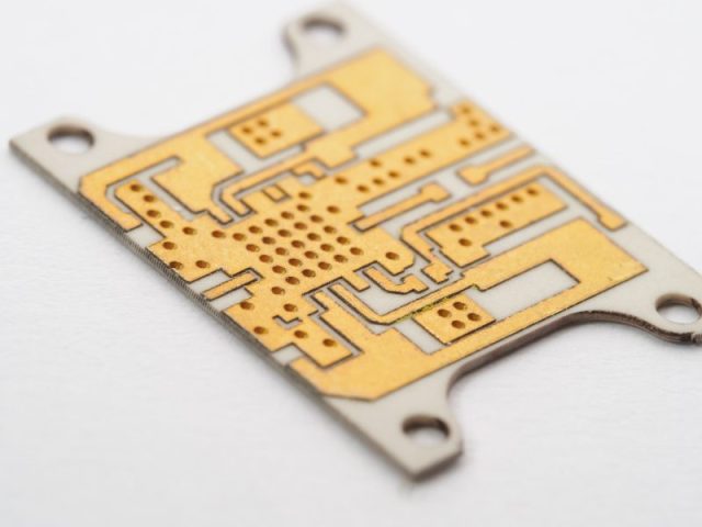
Signal Integrity for High-Frequency Applications:
Low dielectric loss enables stable signal transmission at RF and microwave frequencies. Controlled impedance traces, microstrip or stripline routing, and careful via design reduce reflections and maintain high-frequency performance.
Manufacturing Considerations and QA
Fabricating ceramic PCBs requires specialized processes:
-
Drilling and Metallization: Laser or precision mechanical drilling creates vias without cracking brittle substrates. Copper or gold plating ensures electrical connectivity and solderability.
-
Sintering and Lamination: Ceramic layers are sintered at high temperatures to achieve mechanical strength and dimensional stability.
-
Surface Finishes: Gold, ENIG, or solderable silver are applied for component attachment and reliability.
-
Quality Assurance:
-
Thermal cycling tests confirm mechanical and electrical stability under temperature fluctuations
-
Impedance and continuity testing validate high-frequency and high-current performance
-
AOI and X-ray inspections detect defects and ensure via quality
-
KKPCB applies rigorous process controls and advanced fabrication techniques to deliver high-yield, reliable ceramic PCBs.
Applications of Ceramic PCBs
Ceramic PCBs are used in applications where performance, heat management, and reliability are critical:
-
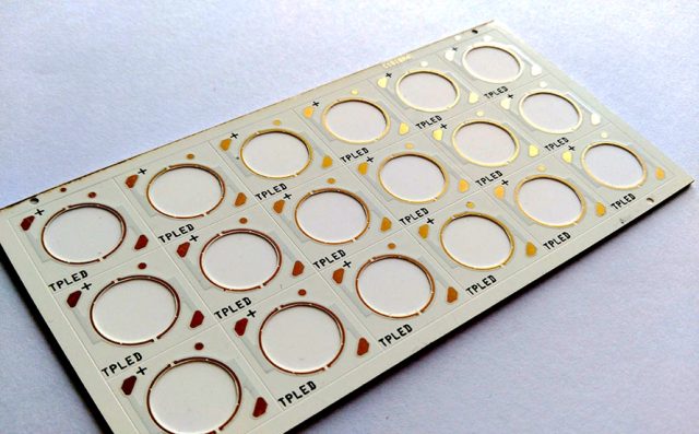
Power Electronics: DC–DC converters, power amplifiers, and LED modules
-
RF & Microwave Devices: Antennas, filters, and high-frequency transceivers
-
Aerospace & Defense: Satellite systems, radar electronics, and avionics operating in extreme conditions
-
Medical Equipment: Laser modules, imaging devices, and high-power diagnostic circuits
-
Automotive Electronics: Electric vehicle power modules, inverters, and ADAS components
By combining advanced materials, thermal management solutions, precision layout, and rigorous QA, KKPCB delivers ceramic PCBs optimized for high-power, high-frequency, and high-reliability applications.
