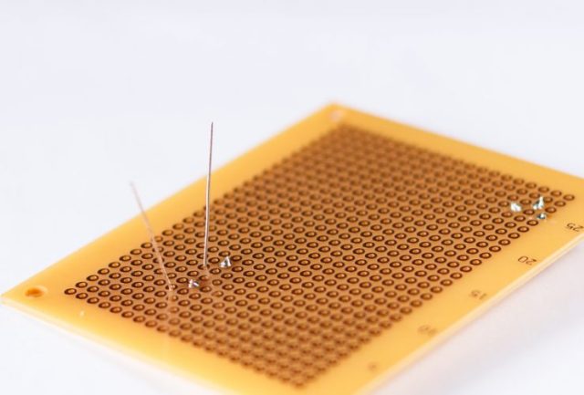
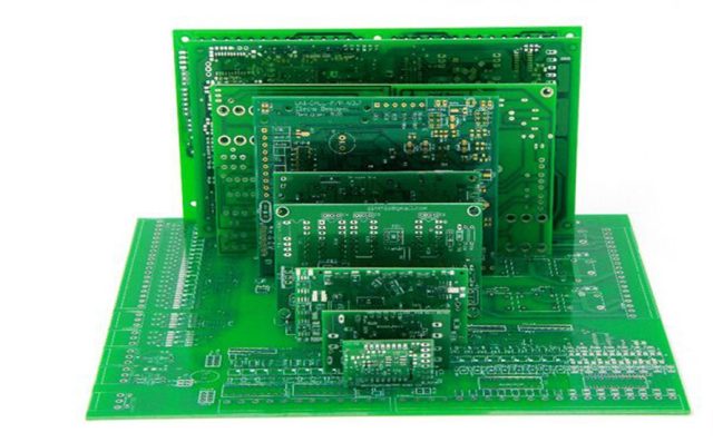
High-precision PCB prototype fabrication has become the backbone of modern electronics development. As product cycles shrink and system complexity rises—spanning RF modules, high-speed digital interfaces, IoT sensors, EV power systems, and aerospace electronics—the demand for PCB prototype accuracy, signal integrity stability, and manufacturing predictability has never been higher.
A high-reliability prototype is not “just a sample”; it is the engineering blueprint that determines whether the final product will meet performance, reliability, safety, and regulatory requirements. When prototypes lack precision, entire projects derail: impedance shifts, EMI failures, timing errors, thermal gradients, and unpredictable field failures.
This is why next-generation products rely on high-precision PCB prototype fabrication technologies—built on advanced materials, micron-scale drilling, controlled impedance modeling, and strict layer-to-layer alignment.
1. Why High-Precision PCB Prototypes Matter for Modern Engineering
Modern electronics integrate high-speed SERDES, RF transceivers, mmWave modules, dense BGA packages, and sensitive analog circuits—all of which require a precision-engineered PCB prototype to validate real-world behavior.
High-precision PCB prototypes ensure:
• Accurate signal propagation
• Predictable impedance profiles
• Stable power delivery networks (PDN)
• Low-noise RF transitions
• Minimal crosstalk across dense routing
• Mechanical and thermal reliability under stress
These qualities directly depend on the fabrication processes used in the prototype stage.
2. Advanced Materials Enable High-Frequency and High-Speed Validation
Prototype reliability begins with material selection. High-precision fabrication supports:
• Low-loss PCB laminates for RF/mmWave systems
• High-Tg FR4 for digital logic and HDI
• PTFE, ceramic-filled, or hydrocarbon composites for GHz-scale performance
• Ultra-smooth copper foils to reduce conductor loss
These materials allow engineers to evaluate insertion loss, phase stability, and EMI behavior long before mass production.
3. Controlled Impedance Fabrication Improves Signal Integrity
With high-speed interfaces such as PCIe Gen5/Gen6, 56G–112G PAM4, and multi-band RF front ends, impedance accuracy becomes essential.
High-precision PCB prototype processes deliver:
• Dielectric thickness tolerance within ±10%
• Trace width/spacing accuracy down to microns
• Uniform copper plating for stable impedance
• Verified microstrip, GCPW, and stripline structures
This guarantees predictable signal integrity, even at multi-gigabit and wideband RF frequencies.
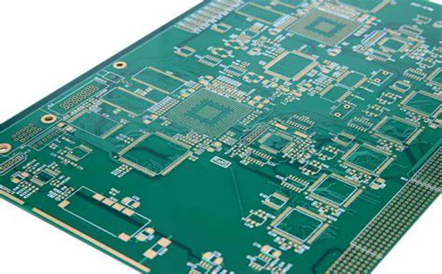
4. HDI, Microvias, and Laser Drilling Enable Dense Routing
Modern prototypes must accommodate 0.4 mm or smaller BGAs, chiplet modules, and highly integrated RFICs.
By using:
• Laser-drilled microvias
• Stacked and staggered HDI via structures
• Via-in-pad to minimize inductive parasitics
• Tight layer-to-layer registration
engineers can test compact, high-density layouts without parasitic effects disrupting RF or digital performance.
5. Surface Finish Precision Shapes RF and High-Speed Behavior
High-precision prototypes use finishes optimized for GHz performance:
• ENIG for reliable BGA solderability
• ENEPIG for wire bonding and RF stability
• Immersion silver for low-loss RF traces
• Hard gold for switch contacts and mechanical wear
Surface uniformity directly impacts conductor loss and signal fidelity.
6. Metrology and Inspection Ensure Prototype Accuracy
State-of-the-art prototype fabrication includes:
• Laser direct imaging (LDI) for accurate patterning
• AOI inspection for trace-level defects
• X-ray via alignment verification
• Cross-section analysis to confirm plating and lamination
These techniques ensure that high-speed and RF designs behave exactly as modeled.
7. Precision PCB Prototypes Reduce Risk in Mass Production
High-precision prototype fabrication allows engineers to:
• Validate design rules
• Verify stackup accuracy
• Confirm EMI/EMC compliance
• Test thermal performance under real load
• Reduce unexpected failures in mass production
A precision prototype is not only a test board—it is the engineering foundation for a stable, scalable manufacturing process.
