PCB Stackup Design & Engineering Services
At KKPCB, we specialize in designing optimized PCB stackups that ensure signal integrity, mechanical stability, and reliable performance in every application. Whether you’re developing high-speed, high-frequency, or complex multilayer boards, our engineering team will guide you through the best layer configuration, impedance modeling, and material selection for your project.
What Is PCB Stackup?
A PCB stackup refers to the arrangement of copper and insulating layers that make up a printed circuit board. Proper stackup design defines how signals, power, and ground layers are structured—minimizing interference, enhancing EMI performance, and improving manufacturability.
Multilayer PCBs typically consist of three or more conductive layers bonded together with insulating prepregs, enabling compact, high-density circuit designs used in modern electronics.
Common Challenges in PCB Stackup Design
While multilayer PCB stacking brings higher performance and integration, it also introduces engineering challenges.
Some typical issues include:
-
Increased EMI Radiation: Poor impedance control can cause reflection and EMI issues. KKPCB uses advanced impedance modeling tools to ensure optimal signal return paths and minimize radiation.
-
Layer Skew: Misalignment during lamination can affect performance. We apply heat staking, rivet, and dowel positioning to maintain perfect layer registration.
-
Stackup Measles: Stress imbalances during pressing may lead to “measles.” KKPCB’s process control adds silicone and epoxy pads to equalize pressure and ensure uniform board thickness.
Five Key Goals for Effective Multilayer Stackups
To achieve stable and high-performance results, every multilayer PCB should strive to meet the following principles:
-
Ground and power planes should be placed as close together as possible.
-
Signal layers should always be adjacent to reference planes.
-
Signal layers should be tightly coupled to their planes.
-
High-speed signals should be routed between planes to control radiation.
-
Multiple ground planes help reduce impedance and electromagnetic emissions.
While an eight-layer board can meet all five principles, KKPCB engineers will help you prioritize the most critical goals for your specific design and cost requirements.
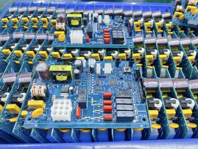
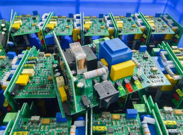
One-Stop PCB & PCBA Service
KKPCB provides global one-stop services covering every stage of your project — from PCB layout, prototype fabrication, and multilayer PCB manufacturing to SMT/DIP assembly, functional testing, final product assembly, and packaging.
Simply send us your Gerber files and BOM list, and our team will deliver high-quality, reliable PCB or PCBA products that meet your exact specifications.
