Why BGA Assembly Is Critical in Modern PCB Design
As electronic devices move toward miniaturization, high-speed performance, and high pin-count integration, the Ball Grid Array (BGA) assembly has become a mainstream packaging technology in:
- Microprocessors (CPU/GPU)
- FPGAs
- High-speed communication ICs
- Memory devices (DDR, LPDDR)
Compared with traditional packages (QFP, SOP), BGA offers:
- Higher I/O density
- Better thermal performance
- Improved electrical performance (shorter signal paths)
However, BGA assembly introduces challenges in PCB design, soldering, inspection, and reliability control.
At KKPCB, BGA assembly is optimized for high yield, reliability, and precision manufacturing.
2. What Is a BGA Package?
2.1 Structure of BGA Package
A Ball Grid Array (BGA) package uses an array of solder balls instead of leads for electrical connection.
Main components:
- Substrate
- Silicon die
- Solder balls (grid array)
- Underfill (optional for reliability)
2.2 Advantages of BGA Packaging
- High pin density
- Compact size
- Excellent heat dissipation
- Reduced inductance → better signal integrity
3. BGA PCB Design Considerations
3.1 PCB Footprint Design
Accurate footprint design ensures:
- Proper solder joint formation
- Reliable electrical connections
Key parameters:
- Pad size and pitch
- Solder mask opening
- Pad finish (ENIG recommended)
3.2 Escape Routing (Fan-Out Design)
Routing signals from BGA pads requires:
- Via-in-pad (VIP) technology
- Microvias (HDI PCB)
- Multi-layer stack-up design
3.3 Controlled Impedance and Signal Integrity
High-speed BGAs require impedance control:
Z0=LCZ_0 = \sqrt{\frac{L}{C}}Z0=CL
Proper routing ensures:
- Minimal signal reflection
- Stable high-speed transmission
- Reduced crosstalk
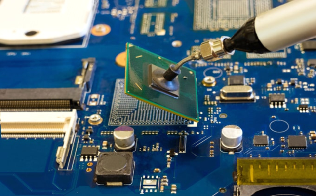
4. BGA Assembly Process
4.1 Solder Paste Printing
- Apply solder paste precisely on PCB pads
- Use stencil with controlled thickness
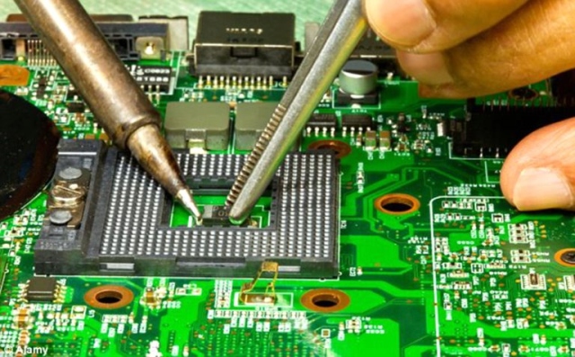
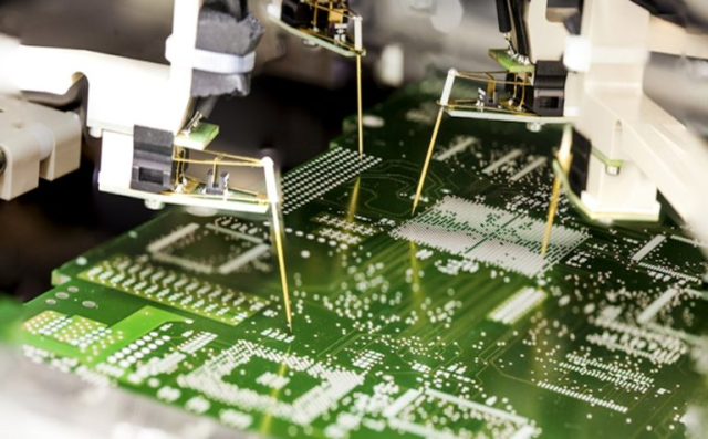
4.2 Component Placement
- High-precision pick-and-place machines
- Accurate alignment of BGA balls with pads
4.3 Reflow Soldering Process
BGA assembly relies on reflow soldering:
- Preheat stage
- Soak stage
- Reflow peak temperature
- Cooling stage
Proper thermal profile ensures:
- Uniform solder melting
- Reliable joint formation
4.4 Cooling and Solidification
Controlled cooling prevents:
- Solder joint stress
- Warpage and defects
5. Inspection and Testing Methods
5.1 X-Ray Inspection
Since solder joints are hidden:
- X-ray is essential
- Detects voids, bridges, misalignment
5.2 Automated Optical Inspection (AOI)
Used for:
- Component alignment
- Surface defects
5.3 Functional Testing
Ensures:
- Electrical connectivity
- System performance
At KKPCB, inspection includes:
- X-ray analysis
- AOI verification
- Functional testing
6. Common BGA Assembly Defects and Solutions
6.1 Solder Voids
Cause:
- Improper reflow profile
Solution: - Optimize temperature profile
6.2 Solder Bridging
Cause:
- Excess solder paste
Solution: - Improve stencil design
6.3 Cold Solder Joints
Cause:
- Insufficient heating
Solution: - Adjust reflow temperature
6.4 Head-in-Pillow (HIP) Defect
Cause:
- Warpage or oxidation
Solution: - Improve process control and storage conditions
7. Reliability Enhancement Techniques
7.1 Underfill Application
Underfill improves:
- Mechanical strength
- Thermal cycling reliability
7.2 Thermal Management
- Heat dissipation design
- Thermal vias under BGA
7.3 PCB Warpage Control
- Proper stack-up design
- Balanced copper distribution
8. Applications of BGA Assembly
BGA assembly is widely used in:
- Consumer electronics (smartphones, laptops)
- High-speed communication devices
- Automotive electronics
- Industrial control systems
- Aerospace electronics
9. KKPCB BGA Assembly Capability
At KKPCB, services include:
- HDI PCB fabrication with microvias
- High-precision BGA placement
- Advanced reflow soldering control
- X-ray inspection and quality assurance
- High-yield mass production
This ensures:
- Reliable solder joints
- Stable electrical performance
- High manufacturing yield
10. Conclusion
BGA assembly is a critical technology in modern high-density and high-speed PCB design, offering superior electrical and thermal performance.
However, achieving reliable BGA assembly requires careful attention to:
- PCB footprint and routing design
- Soldering process control
- Inspection and defect prevention
- Reliability enhancement techniques
With advanced PCB assembly expertise, KKPCB delivers high-quality, high-reliability BGA solutions for global electronics applications.
