
PCB wiring is one of the most critical stages in printed circuit board design. A well-planned routing strategy directly affects signal quality, power stability, electromagnetic compatibility, and manufacturing reliability.
As electronic products continue developing toward:
- Higher operating frequencies
- Smaller form factors
- Greater circuit density
- Increased functional integration
traditional wiring methods are no longer sufficient for modern PCB requirements.
Poor PCB routing may lead to:
- Signal interference
- Voltage instability
- Excessive electromagnetic radiation
- Thermal problems
- Manufacturing difficulties
Therefore, following proper PCB wiring rules is essential for achieving stable and reliable electronic systems.
1. Importance of Proper PCB Wiring Design
1.1 Ensuring Signal Integrity
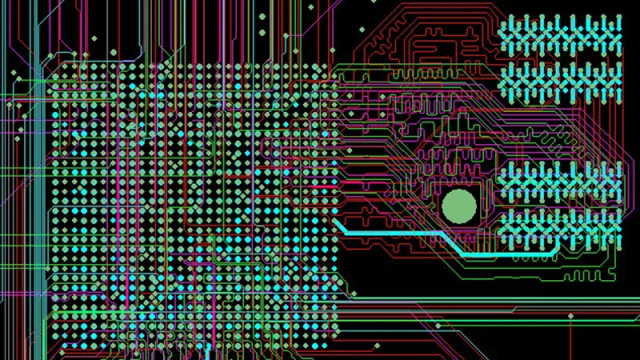
PCB traces are not only electrical connections but also transmission paths for signals.
Improper routing can cause:
- Signal reflection
- Crosstalk
- Signal attenuation
- Timing errors
This is especially important for:
- High-speed digital circuits
- RF circuits
- Communication interfaces
1.2 Improving Power Stability
Power traces carry current to different components.
Poor power routing may result in:
- Voltage drop
- Excessive heating
- Power noise
A proper power distribution network helps maintain stable operation.
1.3 Reducing EMI Problems
Uncontrolled current loops and improper routing structures can increase electromagnetic interference.
Good wiring practices help:
- Reduce radiation
- Improve EMC performance
- Increase system reliability
2. Basic PCB Wiring Rules
2.1 Keep Signal Paths Short and Direct
Shorter routing paths generally provide better electrical performance.
Benefits include:
- Lower signal loss
- Reduced parasitic effects
- Improved transmission stability
Critical signals should avoid:
- Unnecessary detours
- Excessive vias
- Long parallel routing
2.2 Follow the Principle of Functional Block Layout
PCB routing should follow the circuit structure.
Typical functional areas include:
- Power section
- Digital processing section
- Analog section
- RF section
Keeping related circuits together helps reduce interference and simplifies routing.
2.3 Avoid Sharp 90-Degree Corners
Sharp corners can create:
- Impedance discontinuity
- Signal reflection
- Manufacturing stress
Recommended methods:
- 45-degree routing
- Curved traces for high-frequency applications
2.4 Maintain Proper Trace Spacing
Spacing between traces affects:
- Crosstalk
- Signal coupling
- Manufacturing reliability
High-speed and sensitive signals require greater spacing control.
3. High-Speed Signal Routing Rules
3.1 Use Controlled Impedance Routing
High-speed signals require accurate impedance control.
Factors affecting impedance include:
- Trace width
- Copper thickness
- Dielectric thickness
- PCB material
Common impedance requirements include:
- 50Ω single-ended impedance
- 90Ω/100Ω differential impedance
3.2 Maintain Differential Pair Consistency
Differential pairs are widely used in:
- USB
- Ethernet
- PCIe
- LVDS
- MIPI interfaces
Important design practices:
- Maintain constant spacing
- Match trace lengths
- Avoid unnecessary layer changes
3.3 Minimize Signal Return Path Disruption
High-speed signals rely on continuous return current paths.
Avoid routing signals across:
- Ground plane gaps
- Split power planes
- Poor reference structures
A stable return path helps reduce:
- EMI
- Signal distortion
4. Power and Ground Routing Guidelines
4.1 Use Wide Traces for Power Lines
Power traces should be designed according to:
- Current requirements
- Temperature rise limits
- Copper thickness
Insufficient width may cause:
- Overheating
- Voltage drop
- Reliability issues
4.2 Use Ground Planes Whenever Possible
A continuous ground plane provides:
- Low impedance return paths
- Better noise control
- Improved signal integrity
Ground planes are especially important for:
- High-speed circuits
- RF designs
- Mixed-signal systems
4.3 Optimize Decoupling Capacitor Routing
Decoupling capacitors should be placed:
- Close to IC power pins
- With short connection paths
Good routing practices include:
- Short power loops
- Direct ground connections
- Proper via placement
5. Analog and Digital Signal Separation
5.1 Separate Sensitive Analog Circuits
Analog signals are vulnerable to noise from:
- Digital switching
- Power circuits
- Clock signals
Sensitive analog areas should be isolated from noisy sections.
5.2 Avoid Mixing High-Speed and Low-Level Signals
Examples:
Avoid placing:
- Clock lines near sensor signals
- RF traces near switching power circuits
Proper separation improves system performance.
6. RF PCB Wiring Considerations
6.1 Control RF Trace Geometry
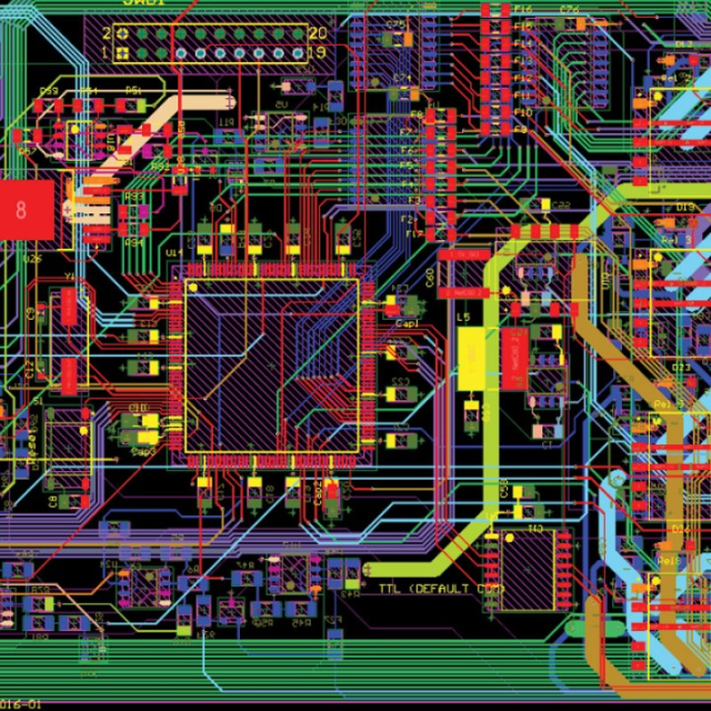
RF traces require strict control of:
- Width
- Length
- Reference plane
- Impedance
Common RF transmission structures include:
- Microstrip
- Stripline
6.2 Keep RF Paths Short
Long RF traces increase:
- Insertion loss
- Phase variation
- Signal attenuation
RF components should be placed close together.
6.3 Use Ground Via Stitching
Via stitching around RF structures helps:
- Improve shielding
- Reduce electromagnetic leakage
- Maintain signal integrity
7. Thermal Considerations During PCB Routing
7.1 Avoid Excessive Current Density
High-current areas require:
- Wider copper traces
- Larger copper areas
- Thermal management structures
7.2 Use Thermal Vias
Thermal vias help transfer heat between PCB layers.
Applications include:
- Power ICs
- LED drivers
- Voltage regulators
7.3 Consider Component Heat Distribution
Heat sources should be identified early.
Examples:
- Power modules
- MOSFETs
- Regulators
Proper placement improves:
- Cooling efficiency
- Product lifetime
8. PCB Wiring Rules for Manufacturability
8.1 Consider PCB Fabrication Capabilities
Design should match manufacturing capabilities.
Important factors include:
- Minimum trace width
- Minimum spacing
- Via size
- Layer alignment
8.2 Avoid Overly Complex Routing Structures
Excessive complexity may increase:
- Manufacturing difficulty
- Production cost
- Failure risk
A balance should be maintained between:
- Electrical performance
- Manufacturing feasibility
8.3 Perform DFM Review Before Production
Design for Manufacturing (DFM) analysis helps identify:
- Routing issues
- Assembly risks
- Reliability concerns
Early review improves:
- First-pass yield
- Production efficiency
9. Common PCB Wiring Mistakes
Long and Uncontrolled Signal Routing
Problem:
Excessive trace length.
Impact:
- Signal delay
- Increased loss
Poor Ground Design
Problem:
Interrupted return paths.
Impact:
- EMI problems
- Signal instability
Incorrect Trace Width Selection
Problem:
Trace cannot support required current.
Impact:
- Overheating
- Reliability failure
Ignoring Manufacturing Limitations
Problem:
Design exceeds fabrication capability.
Impact:
- Low yield
- Increased production cost
10. Recommended PCB Wiring Workflow
Step 1: Analyze Circuit Requirements
Identify:
- Signal types
- Current requirements
- Frequency range
Step 2: Define PCB Stack-Up
Determine:
- Signal layers
- Ground planes
- Power layers
- Material selection
Step 3: Place Critical Components
Prioritize:
- Processors
- Memory
- RF modules
- Power devices
Step 4: Route Critical Signals First
Start with:
- High-speed signals
- Differential pairs
- Sensitive analog paths
Step 5: Perform Design Verification
Check:
- Signal integrity
- Power integrity
- Thermal performance
- Manufacturability
Conclusion
PCB wiring is not simply the process of connecting components; it is a comprehensive engineering task involving electrical performance, signal integrity, thermal management, and manufacturing requirements.
Following proper PCB wiring rules helps engineers achieve:
- Stable signal transmission
- Reliable power delivery
- Reduced EMI risks
- Improved manufacturing yield
As electronic systems continue becoming faster and more compact, optimized PCB routing strategies will remain essential for developing high-performance and reliable electronic products.
