
With the increasing complexity of modern electronic systems, multi-layer PCB boards have become widely used in applications requiring high-density routing, high-speed signal transmission, and improved electrical performance.
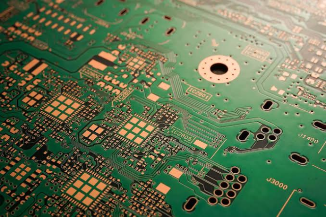
In multi-layer PCB design, grounding is not simply a connection between components and the power supply reference. A properly designed grounding structure directly affects signal integrity, electromagnetic compatibility (EMC), power integrity, and overall system reliability.
As operating frequencies continue to increase, improper grounding methods may lead to issues such as:
- Signal interference
- Ground bounce
- Electromagnetic radiation
- Crosstalk
- Unstable circuit operation
Therefore, selecting an appropriate grounding method and optimizing the ground structure are essential steps in multi-layer PCB design.
1. The Importance of Grounding in Multi-Layer PCB Design
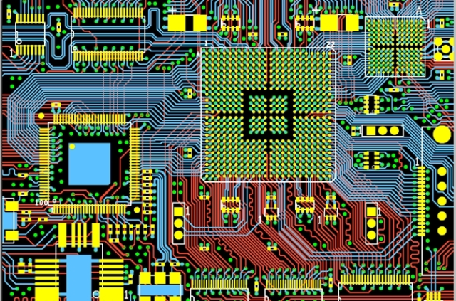
In a PCB system, ground provides a reference potential and a return path for current flow.
For low-frequency circuits, grounding problems may not be obvious. However, in high-speed digital, RF, and power electronics applications, current return paths become critical.
A well-designed grounding structure helps:
- Reduce return path impedance
- Improve signal integrity
- Minimize EMI emissions
- Stabilize power distribution
- Enhance circuit reliability
In multi-layer PCB boards, dedicated ground layers provide advantages that are difficult to achieve with single-layer or double-layer structures.
2. Common Grounding Structures in Multi-Layer PCBs
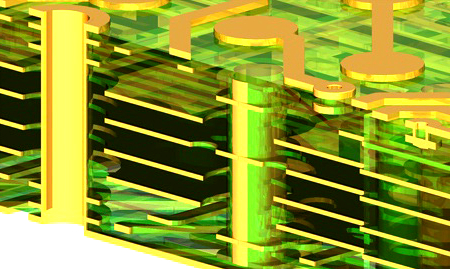
2.1 Dedicated Ground Plane Layer
A dedicated ground plane is one of the most common grounding methods in multi-layer PCB design.
In this structure, one or more internal layers are assigned as continuous ground planes.
Advantages:
- Provides low-impedance return paths
- Reduces electromagnetic interference
- Improves high-speed signal performance
- Supports controlled impedance design
For high-speed PCB applications, placing signal layers adjacent to ground planes helps maintain stable transmission line characteristics.
Common applications include:
- Communication equipment
- High-speed computing systems
- Industrial controllers
- RF circuits
3. Single Ground Plane Method
The single ground plane method uses one continuous ground layer shared by different circuit sections.
This approach is suitable for many general-purpose multi-layer PCB designs.
Advantages:
- Simple structure
- Easy manufacturing
- Good overall grounding performance
However, designers should consider current flow carefully.
If high-noise circuits and sensitive analog circuits share the same ground path, unwanted interference may occur.
Proper component placement and routing strategies are required to minimize noise coupling.
4. Analog and Digital Ground Separation
Many electronic systems contain both analog and digital circuits.
Digital circuits generate switching noise, while analog circuits often require low-noise reference environments.
A common grounding strategy is separating:
- Analog ground (AGND)
- Digital ground (DGND)
These grounds may be connected at a carefully selected point to prevent unwanted current circulation.
Benefits:
- Reduces digital noise interference
- Improves analog measurement accuracy
- Enhances system stability
However, unnecessary ground separation may create longer return paths and increase EMI problems.
Therefore, separation should be based on actual current flow analysis rather than simply dividing areas.
5. Star Grounding Method
Star grounding connects multiple ground branches to a common grounding point.
This method is mainly used in circuits where minimizing ground interaction is important.
Typical applications include:
- Precision measurement equipment
- Audio circuits
- Analog control systems
Advantages:
- Reduces ground loop risks
- Prevents interference between functional blocks
- Improves signal accuracy
Limitations:
For high-frequency circuits, long star connections may introduce additional inductance and are usually less suitable.
6. Ground Via Design in Multi-Layer PCB Boards
Ground vias are essential components for connecting different ground layers.
Proper via design helps maintain continuous grounding paths.
Important considerations include:
Via Placement
Ground vias should be placed:
- Near high-speed signal transitions
- Around RF components
- Near power return paths
This helps reduce unwanted current loops.
Via Array Design
Multiple ground vias can reduce impedance and improve high-frequency grounding performance.
Applications include:
- RF shielding
- Thermal dissipation
- High-current grounding
7. Grounding Considerations for High-Speed Signals
In high-speed PCB design, signal traces require stable return paths.
When a signal crosses:
- Split ground planes
- Layer transitions
- Reference plane gaps
the return current may be interrupted.
This can cause:
- Impedance discontinuity
- Signal reflection
- Increased EMI
Recommended practices include:
- Keep signal layers close to reference planes
- Avoid unnecessary plane gaps
- Add stitching vias when required
- Maintain continuous ground reference
8. Grounding Methods for RF and Microwave PCBs
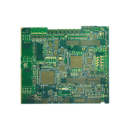
RF circuits have stricter grounding requirements due to high-frequency electromagnetic effects.
Common methods include:
Ground Via Fences
A series of ground vias placed along RF transmission lines can:
- Reduce signal leakage
- Improve shielding
- Control electromagnetic fields
Large Ground Areas
RF circuits often require sufficient ground copper areas to provide stable reference conditions.
Short Return Paths
At microwave frequencies, even small loop areas can affect performance.
Therefore, minimizing current loops is essential for:
- Low signal loss
- Stable impedance
- Reduced radiation
9. Common Grounding Problems in Multi-Layer PCB Design
9.1 Poor Ground Plane Design
Insufficient ground areas or fragmented planes may lead to:
- Increased noise
- EMI issues
- Signal degradation
9.2 Excessive Ground Splitting
Unnecessary separation of ground areas may interrupt return current paths.
This can negatively affect high-speed signal transmission.
9.3 Incorrect Via Placement
Poorly positioned grounding vias may increase:
- Return path length
- Parasitic inductance
- High-frequency losses
10. Manufacturing Considerations for Grounding Design
Grounding performance is not only determined by PCB layout but also influenced by manufacturing processes.
Important factors include:
Layer Stack-Up Control
A stable stack-up ensures:
- Consistent impedance
- Reliable ground reference
- Better electrical performance
Copper Thickness Control
Copper thickness affects:
- Current carrying capability
- Resistance
- Thermal performance
PCB Fabrication Accuracy
Manufacturing variations in:
- Layer alignment
- Etching accuracy
- Via formation
may influence grounding performance, especially in high-frequency applications.
Conclusion
Grounding is a fundamental aspect of multi-layer PCB design that directly influences signal integrity, EMI performance, and system reliability.
Selecting the appropriate grounding method requires consideration of circuit type, operating frequency, current flow, and application requirements.
From dedicated ground planes and ground via optimization to RF grounding techniques, effective grounding strategies help engineers achieve stable and reliable PCB performance.
As electronic systems continue moving toward higher speeds and greater integration, optimized grounding design will remain a key factor in successful PCB development from prototype validation to mass production.
