
With the rapid development of electronic systems toward higher speed, higher integration, and greater functional complexity, PCB reliability has become a critical consideration in high-speed PCB design.
In high-speed applications, PCB performance is influenced not only by signal integrity and impedance control but also by long-term reliability under different operating conditions.
A high-speed PCB must maintain stable performance while facing challenges such as:
- High-frequency signal transmission
- Thermal cycling
- Mechanical stress
- Power fluctuations
- Environmental exposure
- Long-term operation
Poor reliability design may lead to:
- Signal degradation
- Intermittent failures
- Via cracking
- Layer delamination
- Reduced product lifetime
Therefore, PCB reliability design should be considered from the early stages of:
- Material selection
- Stack-up design
- Layout optimization
- Manufacturing process control
- Testing and validation
This article explains the key principles of PCB reliability design in high-speed electronic systems.
1. Importance of PCB Reliability Design in High-Speed Applications
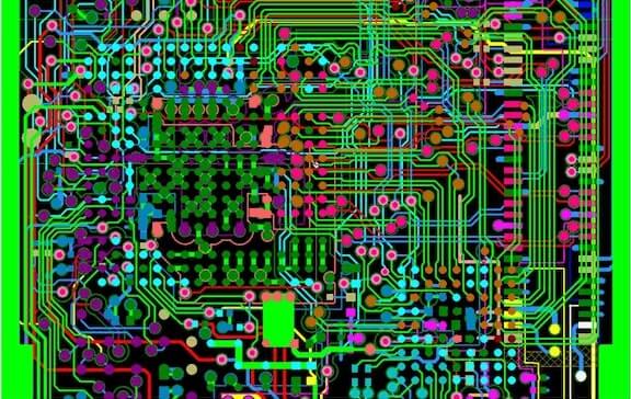
Traditional PCB design mainly focuses on whether circuits can function correctly. However, high-speed PCB design requires additional attention to:
- Electrical performance stability
- Mechanical durability
- Thermal reliability
- Manufacturing consistency
As signal speeds increase, even small physical changes may affect performance.
For example:
- A slight impedance variation may cause signal reflection
- Thermal expansion may damage vias
- Material changes may affect signal transmission
Therefore, reliability design ensures that the PCB can maintain stable operation throughout its expected lifetime.
2. PCB Material Selection for Reliability
The PCB substrate directly affects:
- Thermal performance
- Mechanical strength
- Electrical stability
- Environmental resistance
2.1 Selecting Suitable Dielectric Materials
High-speed PCBs often require materials with:
- Stable dielectric constant (Dk)
- Low dissipation factor (Df)
- Low signal loss
- Low moisture absorption
Common materials include:
Proper material selection helps maintain:
- Controlled impedance
- Signal integrity
- Long-term reliability
2.2 Thermal Expansion Control
The coefficient of thermal expansion (CTE) affects PCB reliability.
During operation and reflow soldering, PCB materials expand and contract.
Excessive expansion differences between materials may cause:
- Via cracks
- Layer separation
- Solder joint stress
High-reliability PCB designs require materials with compatible thermal characteristics.
3. Reliable PCB Stack-Up Design
A well-designed stack-up is essential for both electrical performance and mechanical reliability.
Important considerations include:
- Layer balance
- Material distribution
- Signal reference planes
- Power and ground plane arrangement
3.1 Balanced Layer Structure
An unbalanced multilayer PCB stack-up may result in:
- PCB warpage
- Mechanical stress
- Assembly problems
A balanced structure helps improve:
- Dimensional stability
- Manufacturing yield
- Product reliability
3.2 Proper Power and Ground Plane Design
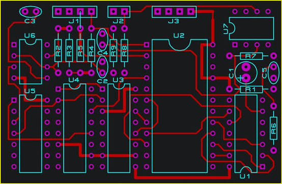
High-speed systems require stable power distribution.
Dedicated power and ground planes help:
- Reduce noise
- Provide return current paths
- Improve EMI performance
A continuous reference plane also improves:
- Signal integrity
- System stability
4. Via Reliability Design
Vias are critical connection structures in multilayer PCBs.
However, they are also common reliability risk points.
Potential failures include:
- Barrel cracks
- Pad cracking
- Poor copper plating
- Thermal stress damage
4.1 Via Structure Selection
Different applications may require:
Through-Hole Vias
Advantages:
- Strong mechanical reliability
- Cost-effective
Applications:
- Standard multilayer PCBs
Blind and Buried Vias
Advantages:
- Higher routing density
- Reduced layer transitions
Applications:
- HDI PCBs
- Compact high-speed designs
Microvias
Advantages:
- Fine-pitch capability
- Improved high-density routing
Applications:
- Advanced electronic products
4.2 Via Manufacturing Control
Reliable vias require control of:
- Hole drilling accuracy
- Copper plating thickness
- Aspect ratio
- Thermal stress resistance
Manufacturing quality directly affects long-term PCB reliability.
5. Signal Integrity and Reliability Design
High-speed PCB reliability is closely related to signal quality.
Important factors include:
- Impedance consistency
- Crosstalk control
- Return path design
- Transmission loss
5.1 Controlled Impedance Design
Impedance variation may cause:
- Signal reflection
- Timing errors
- Communication failures
Key control parameters include:
- Trace width
- Copper thickness
- Dielectric thickness
- Material properties
Manufacturers often use TDR testing to verify impedance performance.
5.2 Reduce Crosstalk
High-speed signals can interfere with nearby traces.
Crosstalk reduction methods include:
- Increasing trace spacing
- Using ground shielding
- Optimizing routing layers
- Controlling parallel trace length
5.3 Maintain Proper Return Paths
High-frequency currents follow the path of least impedance.
Design recommendations:
- Keep reference planes continuous
- Avoid unnecessary plane splits
- Minimize return path changes
Poor return paths may cause:
- EMI problems
- Signal distortion
- Increased noise
6. Thermal Reliability Design
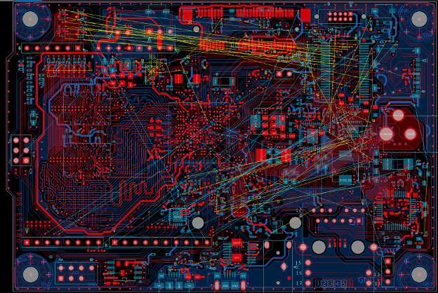
Heat is one of the major factors affecting PCB lifetime.
High-speed systems often contain:
- High-performance processors
- Power management circuits
- RF components
6.1 Thermal Management Methods
Common solutions include:
Increasing Copper Area
Benefits:
- Better heat spreading
- Lower temperature rise
Thermal Vias
Thermal vias transfer heat between PCB layers.
Applications:
- Power components
- High-current circuits
Metal Core PCB Technology
For applications requiring higher heat dissipation:
- Aluminum PCB
- Copper core PCB
may be considered.
7. Power Integrity and Reliability Design
Stable power delivery is essential for high-speed electronic systems.
Power integrity issues may cause:
- Voltage fluctuations
- System instability
- Component failures
7.1 Power Distribution Network (PDN) Optimization
A reliable PDN requires:
- Proper plane design
- Low impedance power paths
- Effective decoupling capacitors
7.2 Decoupling Capacitor Placement
Decoupling capacitors should be placed:
- Close to power pins
- With short connection paths
This helps reduce:
- Power noise
- Voltage fluctuation
8. Mechanical Reliability Considerations
PCB reliability is also affected by mechanical factors.
Important considerations include:
- Board thickness
- Mounting structure
- Connector stress
- Vibration resistance
8.1 PCB Warpage Control
PCB warpage may affect:
- SMT assembly
- BGA solder joints
- Mechanical installation
Control methods include:
- Balanced stack-up
- Uniform copper distribution
- Proper material selection
8.2 Connector and Mounting Reliability
Mechanical stress around:
- Connectors
- Screw holes
- Heavy components
should be carefully evaluated.
Solutions include:
- Reinforcement areas
- Additional copper support
- Mechanical stress analysis
9. Manufacturing Process Control for Reliable PCBs
Reliable PCB design must consider manufacturability.
Important manufacturing controls include:
9.1 Copper Thickness Control
Stable copper thickness ensures:
- Current carrying capability
- Reliable signal transmission
9.2 Lamination Process Control
Proper lamination prevents:
- Delamination
- Internal voids
- Layer separation
9.3 Surface Finish Quality
Suitable surface finishes improve:
- Solder reliability
- Corrosion resistance
Common finishes include:
- ENIG
- ENEPIG
10. PCB Reliability Testing
Before mass production, reliability testing helps verify PCB performance.
10.1 Electrical Testing
Includes:
- Continuity testing
- Insulation testing
- Impedance testing
10.2 Thermal Cycling Testing
Evaluates PCB performance under repeated temperature changes.
Detects:
- Via failures
- Material stress problems
10.3 Mechanical Testing
Includes:
- Vibration testing
- Shock testing
- Bending testing
Important for:
- Automotive electronics
- Aerospace applications
- Industrial equipment
10.4 Environmental Testing
May include:
- Humidity testing
- Corrosion testing
- High-temperature storage
11. Common PCB Reliability Design Mistakes
Ignoring Material Compatibility
Different materials may have different thermal behaviors, causing reliability issues.
Poor Stack-Up Design
An unbalanced stack-up may lead to:
- Warpage
- Mechanical stress
Excessive Via Density
Improper via design may increase:
- Manufacturing difficulty
- Reliability risks
Insufficient Thermal Analysis
Poor thermal design may shorten:
- Component lifetime
- PCB reliability
12. Applications Requiring High-Reliability High-Speed PCBs
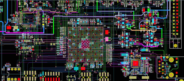
Communication Equipment
Examples:
- 5G systems
- Network infrastructure
Requirements:
- Signal integrity
- Long-term stability
Automotive Electronics
Examples:
- ADAS systems
- Radar modules
Requirements:
- Temperature resistance
- Mechanical reliability
Aerospace Electronics
Examples:
- Satellite systems
- Avionics equipment
Requirements:
- Extreme environment reliability
Semiconductor Equipment
Examples:
- ATE load boards
- Test interface boards
Requirements:
- High-speed accuracy
- Repeatable performance
Conclusion
PCB reliability design is a comprehensive engineering process that combines:
- Material selection
- Stack-up optimization
- Signal integrity control
- Thermal management
- Manufacturing process control
- Reliability testing
For high-speed PCB applications, reliability cannot be achieved through a single design improvement. It requires coordination between PCB designers, engineers, and manufacturers from the earliest development stage.
By applying proper reliability design principles, high-speed PCBs can achieve:
- Stable signal transmission
- Improved production yield
- Longer service life
- Higher system reliability
