
With the rapid development of high-speed electronic systems, PCB designs are facing increasingly complex signal integrity challenges.
Modern electronic devices such as:
- High-speed communication equipment
- Data processing systems
- Automotive electronics
- Industrial control systems
- Semiconductor testing equipment
often operate with high-frequency signals, fast switching speeds, and dense component layouts.
In these environments, signal interference between different circuit sections can seriously affect system performance.
Common problems include:
- Signal crosstalk
- Electromagnetic interference (EMI)
- Timing errors
- Signal distortion
- Communication instability
Therefore, signal isolation technology has become a critical part of high-speed PCB design.
Proper signal isolation helps maintain signal integrity by controlling unwanted coupling between:
- High-speed digital signals
- Analog signals
- Power circuits
- RF circuits
- Sensitive measurement interfaces
This article introduces the key principles, design methods, and practical considerations for signal isolation in high-speed PCB design.
1. What Is Signal Isolation in High-Speed PCB Design?
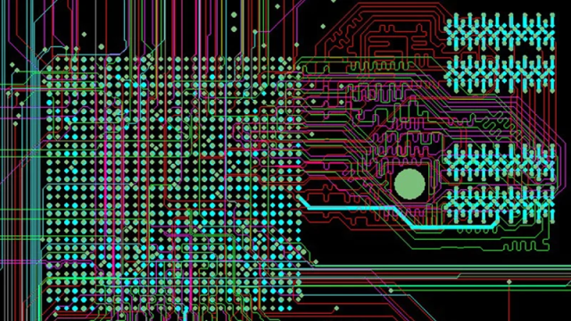
Signal isolation refers to the techniques used to reduce unwanted electrical interaction between different circuits or signal paths.
The main purpose is to prevent:
- Noise transmission
- Electromagnetic coupling
- Ground interference
- Signal degradation
In high-speed PCB design, signals can interact through several coupling mechanisms:
- Capacitive coupling
- Inductive coupling
- Electromagnetic radiation
- Ground bounce
- Power supply noise
Effective isolation design creates controlled electrical environments for different functional areas.
2. Why Signal Isolation Is Important in High-Speed PCBs
2.1 Preventing Signal Crosstalk
Crosstalk occurs when a signal on one trace affects another nearby trace.
It is mainly caused by:
- Excessive parallel routing
- Insufficient trace spacing
- Fast signal transitions
The impact includes:
- False triggering
- Data errors
- Timing instability
Signal isolation reduces coupling by controlling the physical relationship between signal paths.
2.2 Improving Signal Integrity
High-speed signals are sensitive to:
- Voltage fluctuations
- Noise interference
- Impedance changes
Poor isolation can cause:
- Signal reflection
- Overshoot
- Undershoot
- Increased jitter
Proper isolation maintains stable signal transmission.
2.3 Reducing EMI Problems
High-speed switching circuits generate electromagnetic energy.
Without proper isolation, noise may spread through:
- Signal traces
- Power networks
- Ground structures
Good isolation design helps improve:
- Electromagnetic compatibility (EMC)
- System reliability
- Regulatory compliance
3. Main Signal Isolation Methods in PCB Design
3.1 Physical Separation of Functional Blocks
One of the most basic isolation techniques is separating different circuit areas.
Typical PCB partitioning includes:
- Digital circuit area
- Analog circuit area
- Power circuit area
- RF circuit area
For example:
A sensitive analog sensing circuit should not be placed close to:
- Switching power supplies
- High-speed clocks
- Motor drive circuits
Proper functional partitioning reduces noise coupling.
3.2 Ground Plane Isolation
Ground design plays a major role in high-speed PCB performance.
A continuous ground plane provides:
- Low impedance return paths
- Reduced electromagnetic radiation
- Better noise control
For mixed-signal designs, engineers often consider:
- Analog ground
- Digital ground
- Power ground
However, improper ground separation may create additional problems.
The key principle is:
Maintain controlled return current paths instead of simply dividing ground planes.
3.3 Guard Trace Design
Guard traces are additional copper traces placed between sensitive signals.
They are usually connected to ground.
Functions include:
- Reducing capacitive coupling
- Providing electromagnetic shielding
- Protecting sensitive signals
Applications:
- Analog measurement circuits
- Sensor interfaces
- High-impedance signal paths
3.4 Increasing Trace Spacing
Trace spacing is one of the simplest methods to reduce crosstalk.
Increasing distance between signal lines reduces:
- Electric field coupling
- Magnetic field interaction
Important factors include:
- Signal frequency
- Trace length
- Layer structure
- Dielectric thickness
For high-speed differential pairs, spacing must follow controlled impedance requirements.
3.5 Differential Signal Isolation
Differential signaling is widely used in high-speed systems.
Examples:
- USB
- PCIe
- Ethernet
- LVDS
Differential pairs provide:
- Better noise immunity
- Reduced electromagnetic radiation
- Improved signal stability
Design requirements include:
- Matched trace length
- Controlled spacing
- Continuous reference planes
3.6 Via Shielding Technology
Via fences can be used around sensitive signal paths.
A via fence consists of multiple grounded vias placed along a signal boundary.
Advantages:
- Creates electromagnetic barriers
- Reduces signal leakage
- Improves RF isolation
Common applications:
- RF PCB
- Microwave circuits
- High-speed communication boards
3.7 Layer Stack-Up Optimization
A properly designed PCB stack-up improves signal isolation.
Typical high-speed PCB structures include:
Signal Layer Adjacent to Ground Plane
Advantages:
- Controlled impedance
- Short return path
- Reduced EMI
Dedicated Power and Ground Layers
Benefits:
- Stable power distribution
- Reduced noise coupling
Symmetrical Stack-Up
Helps reduce:
- PCB warpage
- Mechanical stress
- Manufacturing variation
4. Signal Isolation Between Different Circuit Types
4.1 Digital and Analog Isolation
Digital circuits generate:
- Switching noise
- Harmonic interference
Analog circuits are sensitive to:
- Small voltage variations
- Noise injection
Design methods:
- Separate placement
- Independent signal routing
- Proper grounding strategy
- Filtering circuits
4.2 Power and Signal Isolation
Power circuits generate:
- Large current changes
- Switching noise
Isolation methods include:
- Separate power routing
- Short current loops
- Proper decoupling capacitor placement
4.3 RF Signal Isolation
RF circuits require strict isolation due to high-frequency characteristics.
Important considerations:
- Controlled impedance traces
- Ground shielding
- Short RF paths
- Proper antenna clearance
Poor RF isolation may result in:
- Reduced transmission range
- Signal loss
- Frequency instability
5. Isolation Design for High-Speed Interfaces
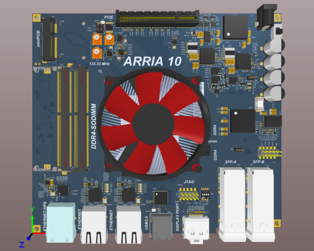
5.1 USB High-Speed Design
Important considerations:
- Differential impedance control
- Short routing distance
- Avoiding unnecessary vias
5.2 Ethernet Interface
Requirements:
- Differential pair matching
- Transformer isolation
- Noise suppression
5.3 PCIe and High-Speed Data Interfaces
Need careful control of:
- Trace length matching
- Reference planes
- Crosstalk
6. Common Signal Isolation Design Mistakes
6.1 Excessive Parallel Routing
Problem:
Long parallel traces increase coupling.
Solution:
- Increase spacing
- Change routing direction
- Add reference shielding
6.2 Splitting Ground Planes Incorrectly
Problem:
Creates discontinuous return paths.
Result:
- Increased EMI
- Signal degradation
Solution:
Use proper return path planning.
6.3 Ignoring Return Current Paths
Problem:
Signals may find unexpected return paths.
Result:
- Noise radiation
- Signal integrity problems
Solution:
Provide continuous reference planes.
6.4 Placing Noisy Components Near Sensitive Circuits
Problem:
Noise sources affect critical signals.
Solution:
Separate according to functional priority.
7. Verification Methods for Signal Isolation
Before production, engineers can evaluate isolation performance through:
Signal Integrity Simulation
Used to analyze:
- Crosstalk
- Reflection
- Signal quality
Electromagnetic Simulation
Used to evaluate:
- Radiation
- Coupling effects
- Shielding effectiveness
Prototype Testing
Common measurements:
- Oscilloscope analysis
- Network analyzer testing
- EMI testing
8. Signal Isolation Considerations During PCB Manufacturing
Signal isolation performance depends not only on design but also manufacturing accuracy.
Important manufacturing factors include:
Impedance Control
Variations in:
- Trace width
- Copper thickness
- Dielectric thickness
can affect isolation performance.
Layer Alignment Accuracy
Misalignment may cause:
- Impedance variation
- Signal coupling changes
Material Selection
High-speed applications may require:
- Low-loss laminates
- Stable dielectric materials
Examples:
- Rogers RO4003C
- Rogers RO4350B
- PTFE-based materials
Conclusion
Signal isolation technology is a fundamental element of high-speed PCB design.
As electronic systems continue moving toward:
- Higher frequencies
- Faster data rates
- Greater integration density
effective isolation strategies become increasingly important.
A successful high-speed PCB design requires comprehensive consideration of:
- Functional partitioning
- Ground design
- Trace spacing
- Differential routing
- Stack-up optimization
- EMI control
By applying proper signal isolation techniques, engineers can reduce interference, improve signal integrity, and achieve more reliable electronic products.
