
Table of Contents
A robot wrist that combines a camera, a force/torque sensor, and a motor interface has three different definitions of “clean data.” The camera needs controlled differential paths and a stable clock; the force sensor needs low-noise bias and reference currents; the motor interface creates fast switching edges and heat. A Robotics PCB must let those domains coexist without turning a lighting change into a force error or a motor command into a vision-data drop.
The project pain usually appears during integration. Each subsystem passes its own bench test, but the assembled wrist loses margin when the camera link is active, the ADC samples, and the joint moves at the same time. The workflow below gives the mixed-signal design a physical partition, an evidence-based test plan, and a manufacturing handoff that a sourcing team can audit.
Why vision and force signals fight on one board
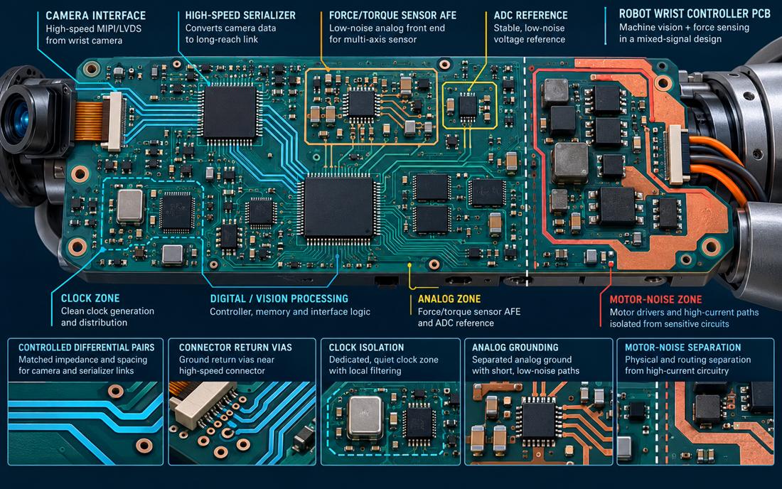
Camera serializers on a Robotics PCB, memory clocks on the Robotics PCB, ADC references, and motor switches share the same enclosure but should not share the same return path. Begin the PCB design review by drawing three current maps: the high-speed camera and memory return, the low-frequency sensor return, and the motor-power return. If they cross at a connector or plane neck, document why; if they can be separated, reserve the geometry before component placement is frozen.
For a Robotics PCB in a wrist module, mechanical constraints often force a long, narrow outline. That makes layer transitions and connector launches more important than an idealized square board. Define the camera connector datum, the force-sensor entry, and the motor-cable exit on the same mechanical view so the layout team does not trade one interface against another late in the project.
Partition clocks, analog, and motor noise
Give the force/torque front end a short, quiet region with its reference, bias network, and ADC pins close together. Keep the clock generator, serializer, and memory on a separate digital island with a continuous return. The motor driver and converter belong near the power entry and should have their own thermal and return strategy. The PCB materials and stackup must be selected before routing because dielectric thickness controls both differential geometry and field coupling between the islands.
Do not use a split plane as a universal answer. A split can force an edge current around a gap and increase coupling. Prefer controlled placement, a continuous reference under the high-speed pair, and a planned single connection between analog and digital references. For sensitive force channels, route the sense pair symmetrically, keep bias currents away from the ADC reference, and prevent motor return vias from landing inside the analog region.
Use controlled impedance as an integration tool
High-speed camera links on a Robotics PCB need a geometry that the fabricator can repeat. Define pair width, spacing, reference layer, via transition, and allowed skew in the release drawing. A high-frequency PCB workflow is useful even when the link is short, because the connector, flex cable, and return vias can dominate the launch. Tie any impedance coupon or acceptance method to the actual product stackup rather than a generic calculator.
Protect high-speed launches
At the camera connector on the Robotics PCB, keep the pair escape short, place return vias beside signal vias, and avoid a copper island that ends under the connector shell. If a flex or coax transition is used, define the mechanical datum and bend keep-out with the electrical launch. The PCB manufacturing drawing should call out drill registration, back-drill or via-in-pad assumptions, solder-mask openings, and inspection access.
The Robotics PCB force sensor connector needs a different treatment. Keep its excitation and sense returns together, protect the input from ESD at the entry point, and make the shield bond part of the enclosure strategy. A shared connector shield can inject a camera common-mode current into the force reference if the chassis path is not intentional.
Calibrate the sensor chain
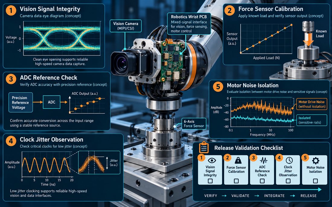
Robotics PCB calibration is more than writing an offset to memory. Apply a documented load to the force sensor, verify the reference and ADC path, and record the board and firmware revision with the result. Exercise the camera link and motor switching while the calibration input is active; otherwise the team may miss a coupling mechanism that appears only in the integrated wrist. Label these as design-verification or engineering-range results, not customer measurements.
Use a Robotics PCB test fixture that can select a known force input, a camera pattern, a clock observation point, and a motor-noise condition. During PCB assembly inspection, verify the sensor connector, reference capacitors, high-speed launch, and thermal interface. If the wrist uses selective coating, keep the sensor contacts and optical connector areas defined in the drawing.
Release a wrist module
Before Robotics PCB release, check that the camera pair has a repeatable launch, the force reference has a named return, the motor domain has a compact high-current path, the connector shields have a defined chassis bond, and the fixture can reproduce the integrated operating state. Use PCB fabrication coupons or sample panels to confirm the stackup and the finish on fine-pitch launches.
A controlled Robotics PCB PCB prototyping build should include the camera cable, sensor, motor harness, and enclosure hardware—not only the bare board. Document PCB finish compatibility, assembly acceptance, and signal integrity evidence in the same revision package. If the board changes outline or connector position, reopen the mixed-signal partition instead of assuming the old test remains valid.
For a production-ready Robotics PCB, the final decision is simple: every interface has a physical return, every calibration value has an owner, and every high-speed or motor change triggers an integrated retest.
Sources: camera-interface, ADC, force-sensor, and serializer manufacturer application notes; Analog Devices guidance on mixed-signal grounding and references; Qorvo and Würth material on controlled returns and EMC; laminate and connector data sheets; and KKPCB capability pages for design, materials, fabrication, assembly, and prototyping. All values are engineering targets or verification practices, not customer test results.
