
Table of Contents
A predictive-maintenance gateway only creates value when its sensor data remains trustworthy after months of vibration, temperature cycling, motor noise, and maintenance activity. A Smart Factory PCB in this role is not simply a carrier for an ADC and a processor.
It is the boundary between a small analog signal—such as bearing vibration, winding temperature, pressure, or current—and the decision to schedule a service visit. The project pain usually appears when a healthy machine begins to look abnormal because the board has allowed ground bounce, reference noise, or connector contamination into the measurement chain.
This article treats the gateway as an engineering release, not a generic IoT node. A second Smart Factory PCB review keeps the sensor evidence tied to the physical board. It explains how to partition the signal path, protect calibration access, control the return current, and give manufacturing and service teams evidence they can use.
Smart Factory PCB Signal Chain: From Symptom to Cause
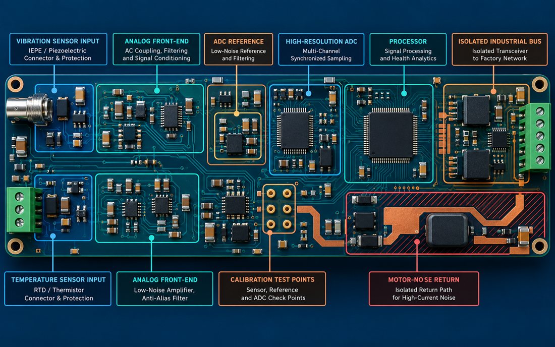
Start with the complete measurement chain: sensor excitation, connector, protection, gain stage, anti-alias filter, ADC reference, processor, isolated communications, and the power converter that feeds them. A project team often debugs the algorithm first, while the real error is a few millivolts of periodic interference coupled from a switching node.
The first design review should therefore map each fault signature through a Smart Factory PCB release map to a physical region of the PCB design: a 50/60 Hz pickup path, a PWM edge, a long shield drain, or a return current forced through the reference area.
For a Smart Factory PCB vibration input, preserve the sensor’s source impedance and keep the protection network from adding an uncontrolled pole. For a thermistor or RTD, route the sense pair as a defined differential path and keep its bias current away from digital return vias.
For a current transformer or Hall sensor, reserve a short, symmetrical path into the amplifier. These choices let firmware distinguish a real machine change from a layout-induced artifact.
Build a quiet analog island
Place the analog front end, reference, and converter pins inside a deliberate quiet island. The island is not an isolated copper “moat” that forces a high-frequency current to detour; it is a controlled partition with one planned return connection and a clear escape path for digital and power currents.
Select suitable PCB materials and stackup geometry for the environment, then define the copper balance and reference planes before routing the sensor channels.
A practical release rule for a Smart Factory PCB is to keep the reference trace short, avoid sharing it with an indicator LED or relay driver, and place its decoupling capacitor at the reference pin rather than at the edge of the board.
Guard rings can help with high-impedance inputs, but they are not a substitute for clean bias-current routing. When the gateway must operate near a VFD or servo drive, use a continuous reference plane, a controlled chassis-to-signal strategy, and a connector shield termination that does not send surge current through the ADC ground.
Partition by current, not by schematic labels
On the schematic, an isolated transceiver may look like a separate block. On the board, its primary-side return, transformer capacitance, and connector shield still create a current path. Keep the isolated interface beside its field connector and keep the noisy converter loop compact.
A high-frequency PCB layout mindset is useful even when the sensor bandwidth is modest, because fast digital edges and converter harmonics still need a low-inductance return.
Keep the edge controller honest
The edge processor normally performs windowing, feature extraction, and alarm decisions. Give it clean supply domains and locate clock, memory, and Ethernet routing away from the analog island. If Ethernet or another high-speed link leaves the enclosure, define the connector datum, magnetics placement, and common-mode path as one design problem.
The manufacturing drawing should call out PCB manufacturing constraints for controlled impedance, drill registration, copper balance, and any press-fit or shield features.
For a gateway that reports a bearing trend, retain raw samples or a diagnostic statistic rather than transmitting only a binary alarm. That makes an intermittent board-level error visible during commissioning. Provide a service header or test pads for the reference, sensor bias, isolated supply, and a known calibration input. Test access is cheaper at layout time than a field return.
Validate drift before deployment
Validation of a Smart Factory PCB should challenge the measurement path in the same sequence the product will experience it: power-up, sensor excitation, motor-noise exposure, thermal soak, connector handling, and communications traffic. Use a calibrated input or a documented simulator; label the result as a design verification value, not as a customer measurement.
A typical engineering target is to keep the zero shift within the project’s error budget after the board reaches thermal equilibrium, while a separate limit covers short transient disturbances.
Measure the reference and analog ground at the connector, amplifier, and ADC—not only at the bench supply. Compare the time correlation between a converter switching edge and the reported sensor feature.
If a channel changes only when an isolated bus transmits, inspect capacitively coupled return current before changing firmware. This Smart Factory PCB evidence helps a project manager decide whether to revise the layout, shielding, or enclosure.

Smart Factory PCB Predictive-Maintenance Release
Before the Smart Factory PCB design enters PCB assembly, freeze a short release checklist: sensor connector pinout and shield bond, analog return boundary, reference decoupling, protection leakage, test-pad access, isolation spacing, and the firmware calibration record. A pilot build for the Smart Factory PCB should verify solderability, connector coplanarity, coating keep-outs, and inspection coverage.
Confirm PCB fabrication registration before the first panel is released. If the board uses a mixed stackup or a dense field connector, ask the fabricator to review the drawing and panelization rather than relying on a generic rule set. A controlled PCB prototyping loop should expose changes before volume tooling.
Use the following decision gates, including PCB finish compatibility and signal integrity PCB review: (1) every sensor channel has a named return path; (2) the ADC reference is measured at the pin; (3) the power converter loop is physically separated from the analog island; (4) calibration can be repeated without removing the board; and (5) the manufacturing package identifies the acceptance method.
The same gates protect a Smart Factory PCB sourcing decision: document the RF PCB return path and the assembly process used for calibration access. a second supplier can quote the design without silently changing the dielectric, copper balance, or test method. Where a redesign is needed, keep the revision tied to the alarm model and to the dielectric material actually released so a data change can be traced to a physical change.
Sources: Taconic and other laminate manufacturer data sheets for dielectric and thermal guidance; Analog Devices application material on precision signal chains and grounding; Qorvo and Würth engineering resources for RF/EMC layout principles; and KKPCB capability pages for design, material, fabrication, and assembly planning.
Values in this article are typical engineering targets or design-review ranges, not customer test results.
