
In an Industrial IoT PCB review, the PoE path should be treated as both a power interface and a measurement reference. The placement decision affects cable noise, sensor repeatability, and service access long after the prototype leaves the lab.
Power over Ethernet makes an industrial edge node easier to install, but it also concentrates magnetics, conversion loss, cable transients, and sensor electronics on one compact assembly. A reliable Industrial IoT PCB must route the powered link, control the transformer and converter heat, and keep the sensor reference explainable when the enclosure is closed. The design challenge is not simply delivering power; it is releasing a board whose electrical, thermal, and manufacturing interfaces stay aligned.
- Define the PoE entry and magnetics region before placing the sensor channel.
- Give the power stage a deliberate copper and enclosure heat path.
- Keep network return and sensor reference from sharing uncontrolled current.
- Validate powered operation with thermal probes and revision-controlled records.
Place PoE entry, magnetics, and sensor zones as one system
Begin with the connector, magnetics, protection parts, and isolation boundary. The PCB design should show the powered-pair path, chassis or shield datum, and the first reference plane transition. A sensor port placed beside the magnetics may see magnetic or thermal coupling even when the nets are unrelated. The Industrial IoT PCB stackup needs enough reference continuity for the Ethernet path while leaving a practical area for thermal spreading.
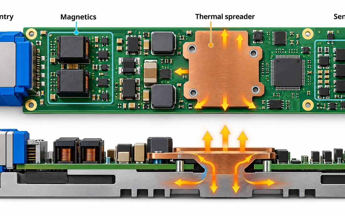
Keep the connector launch and magnetics footprint close enough to control the return path, but do not let a copper heat spreader extend into a sensitive sensor zone without an explicit reason. The high-frequency PCB rules should cover the Ethernet pair and clock transitions; the mechanical drawing should cover connector shell, shield, and enclosure contact.
Make the heat path visible in the fabrication package
PoE magnetics, rectifiers, and DC/DC stages can create a local hot region. The PCB manufacturing release should identify copper weight, thermal vias, spreader geometry, and any keep-out that protects a sensor or polymer connector. A nominal laminate substitution can change dielectric spacing and thermal behavior, so the PCB materials list must stay tied to the released stackup.
| PoE region | Engineering risk | Release evidence |
|---|---|---|
| Powered entry | Cable surge or shield-current coupling | Connector and protection overlay |
| Magnetics | Magnetic and thermal interaction | Placement, height, and keep-out notes |
| Power stage | Heat and switching noise | Copper, via, and enclosure heat path |
| Sensor port | Drift or blocked service access | Port, probe, and fixture datum |
The PCB assembly drawing should call out magnetics orientation, polarity, shield hardware, thermal interface material, and any masked sensor opening. Those details cannot be recovered from a bare netlist after the board is built.
Validate powered operation under thermal and cable conditions
A powered-link test should include the intended cable, connector torque, enclosure support, and airflow direction. The assembly fixture needs a board datum and probe access at the magnetics, power stage, and sensor reference. Treat a test setup as a method definition, not as a customer measurement; record the fixture revision, board revision, cable family, and acceptance method.
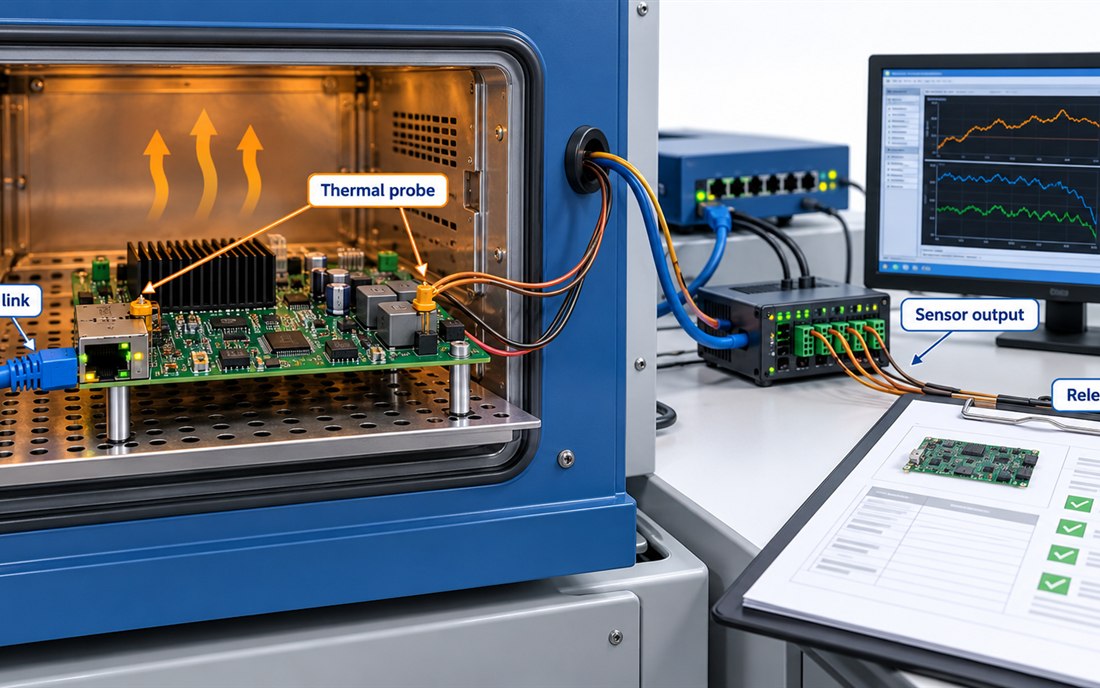
The PCB fabrication traveler should keep panel orientation, copper-balance notes, coating instructions, and inspection access together. If an enclosure or heat sink changes, repeat the fixture check before assuming the earlier result transfers. A design target, a typical material value, and a measured production result must remain separate in the record.
Change-control questions for an Industrial IoT PCB PoE release
- Did the cable, connector, magnetics, or powered-pair path change?
- Did the converter, thermal spreader, or enclosure airflow change?
- Did the sensor port, coating mask, or probe datum move?
- Did the stackup, copper weight, or approved laminate change?
- Did firmware timing alter the powered load or sensor sampling window?
A production Industrial IoT PCB release should make the PoE heat path and sensor reference visible to engineering, assembly, and procurement. The thermal layout, the fabrication release, and the assembly traveler should share the same board and fixture identifiers.
For procurement, approve the Industrial IoT PCB and Industrial IoT PCB only with the connector, magnetics, and thermal assumptions attached. That keeps a substitute component from turning into an untracked sensor or Ethernet problem.
An Industrial IoT PCB release is ready only when the powered link, thermal path, and sensor reference are reviewed together. This combined check prevents a late connector or enclosure change from reopening EMC and calibration work.
Sources: Analog Devices Ethernet, power-integrity, and sensor guidance; Würth Elektronik grounding, magnetics, and assembly notes; Qorvo interface references; PoE controller, connector, magnetics, coating, and PCB material supplier application data. Checks above are engineering release practices, not customer qualification results.
