
Industrial controllers rarely fail because a schematic is missing a component. They fail after the board is placed in a metal cabinet, a long cable is bonded at the wrong point, or a protective coating covers a connector that still needs a reliable return path. An Industrial IoT PCB for a pump skid, machine vision node, or distributed I/O gateway must survive a mixed environment: fast common-mode transients at the cable entry, low-level sensor signals near switching converters, condensation during a cold start, and service technicians who need to remove the board without damaging its shield bond.
An Industrial IoT PCB review should name the enclosure, cable, and coating assumptions before a buyer freezes the build.
This design review treats the board and enclosure as one electromagnetic and mechanical system. The goal is not to claim a customer qualification result. It is to give an engineer or project manager a release method that can be checked against the actual enclosure, cable, coating, and assembly drawing before a pilot build.
- Place the shield termination and transient zone at the real cable datum.
- Keep sensitive sensor references out of the high-current chassis-return path.
- Define coating keep-outs before copper, connector, and test-point placement are frozen.
- Release assembly and enclosure-fit evidence as one controlled package.
For an Industrial IoT PCB, the enclosure boundary is part of the circuit and must be reviewed before routing is frozen.
Table of contents
Start with the enclosure boundary, not the connector symbol
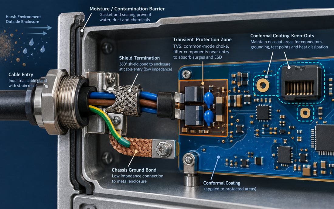
The first mistake on an Industrial IoT PCB is to treat the connector as an electrical symbol and postpone the cabinet interface until mechanical design is complete. In a real panel, the cable gland, shield clamp, mounting screw, and board edge form a short current path. If those features are separated on the drawing, a transient can travel across the signal area before reaching the intended chassis reference.
Build the layout around a measured mechanical datum: the panel cut-out, board mounting hole, and cable-entry centerline. A low-impedance chassis bond should be shorter and wider than the ordinary digital return. Where the enclosure is painted, define a controlled bare-metal contact or a dedicated grounding washer; do not assume that a mounting screw through powder coat is an RF bond. The PCB materials selection also matters because resin, copper balance, and finish behavior affect drilling, coating adhesion, and the long-term stability of the interface.
Separate three return paths that are often mixed together
A practical enclosure review draws three paths in different colors: the high-current protective or chassis path, the fast common-mode path at the cable entry, and the quiet reference used by sensors and converters. They may meet at a controlled point, but they should not share a narrow neck of copper. A high-frequency PCB treatment is useful even when the product is not a radio because the edge of a fast industrial cable event has high-frequency content.
Place TVS devices, common-mode chokes, and connector-to-chassis capacitors according to the current path, not according to the order in the schematic. The component that is electrically first but physically far away is not first during a surge. A short, wide copper region with stitching to the chassis reference normally gives the protection network a more predictable impedance than a long trace that crosses the sensor return.
An Industrial IoT PCB can lose EMC margin when a shield is treated as decoration instead of a current path.
Use shielding without creating a new antenna
Shield cans and copper fences are helpful only when their return path is continuous. A fence with a broken row near the connector can leave an aperture exactly where the cable field is strongest. For an Industrial IoT PCB, use a perimeter via pattern that respects drill-to-edge limits, connector keep-outs, and the enclosure screw pattern. Do not place a via under a connector pin or inside a coating keep-out simply to make the fence look symmetrical.
In an Industrial IoT PCB, the cable entry is the first place to compare the electrical intent with the enclosure hardware.
The Industrial IoT PCB cable interface should be checked with the actual gland and clamp, not only a CAD symbol.
At the cable entry, make the 360-degree shield bond the mechanical responsibility of the gland or clamp. On the board, the shield landing, mounting hardware, and return stitching should be documented as separate features. A project manager can then ask the fabricator and assembler the same question: which surface is expected to be conductive after finish, cleaning, and coating? This avoids a late argument in which the schematic says ground, the mechanical drawing says paint, and the assembly traveler says mask.
Protect sensor references from shield-current decisions
Industrial analog channels are vulnerable to reference movement rather than only to radiated noise. Keep ADC references, bridge sensors, and communication isolators away from the shield landing and power-entry copper. Use a quiet copper island only when its connection point is intentional; a floating island can become a capacitive pickup plate. The PCB manufacturing drawing should identify controlled copper areas, via tenting expectations, and any exposed metal that must remain free of coating.
For a mixed-signal gateway, make the reference transition visible in the review package. Show where the isolated side ends, where the cable shield is bonded, and where the enclosure bond is made. If the board uses a high-impedance sensor input, reserve a guard region and test access before routing density forces a compromise. That planning is more useful than simply adding another filter after the prototype is already assembled.
The Industrial IoT PCB coating plan should be released with the connector, test, and service interfaces rather than added as a late manufacturing note.
Design coating keep-outs as functional interfaces
Conformal coating is not a generic green layer applied after assembly. On an Industrial IoT PCB, it is a selective process with edge coverage, viscosity, masking, cure, and rework consequences. Keep connectors, shield springs, chassis pads, probe points, adjustment components, and heat-transfer surfaces clear where their function requires metal-to-metal contact. Give the assembler a keep-out drawing with a measurable boundary, not a note that says do not coat connector area.
When a sensor port needs environmental protection, consider a two-zone approach: a coated component region and a clean service region. The transition should avoid a sharp meniscus over a fine-pitch lead or a vent hole. For high-voltage or isolated nets, the coating can support environmental robustness, but it does not replace the required clearance, creepage, slot, or safety review. These rules belong in the PCB assembly traveler so the operator, inspection technician, and rework technician use the same interpretation.
Check materials and finish compatibility before pilot build
An Industrial IoT PCB coating decision also affects repair strategy, so the release package should define how a damaged area is inspected and restored.
Ask the material and coating suppliers for the applicable compatibility guidance, then validate it against the actual surface finish, flux-cleaning process, and cure profile. The intent is not to copy a supplier curve into the product specification. The intent is to identify risks such as poor adhesion on a contaminated surface, trapped solvent under a connector, or a cure temperature that shifts a sensor calibration. A qualified PCB fabrication partner can help turn those risks into inspection points and sample coupons.
Do not use the coating to hide an unfinished design. If a copper edge, via barrel, or solder joint must carry a mechanical or electrical load, document that function before coating is approved. The same rule applies to the surface finish: select it for the contact, soldering, corrosion, and storage requirements that are actually present, rather than choosing a finish by habit.
When an Industrial IoT PCB moves from prototype to pilot, enclosure fit and electrical evidence must travel in the same revision package.
Release a manufacturing and enclosure-fit package
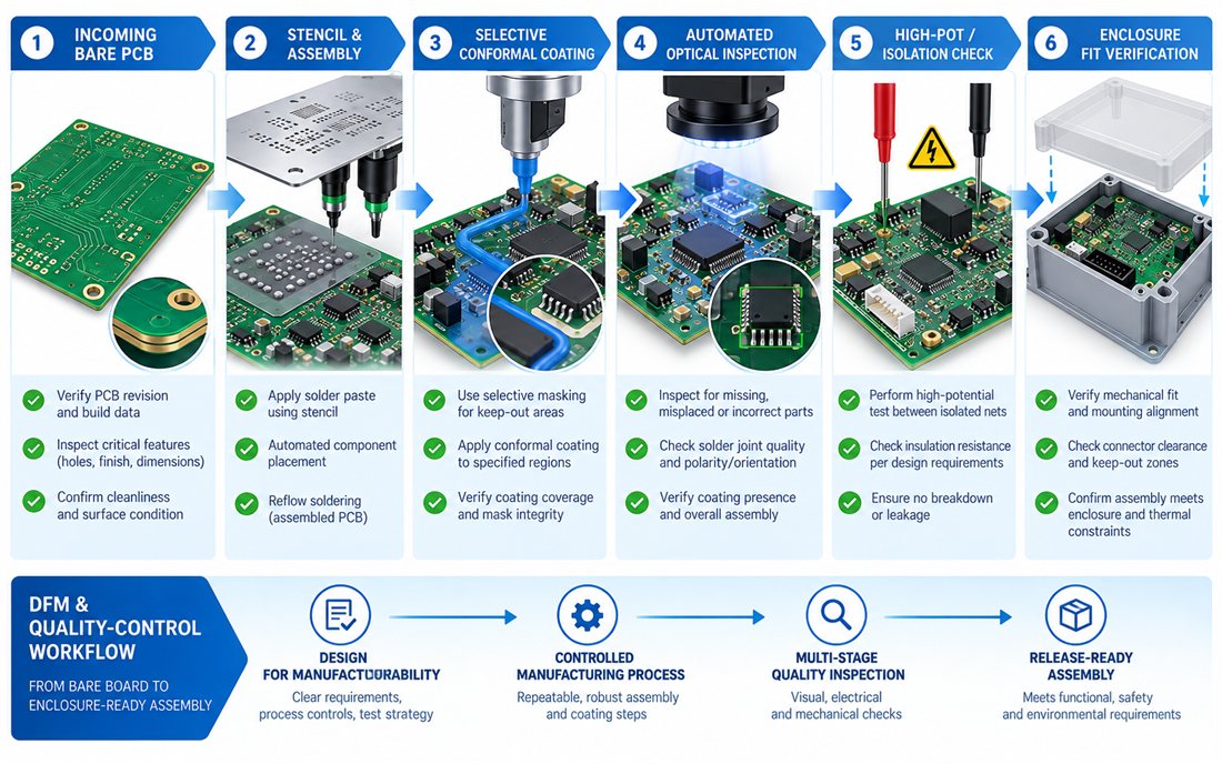
The last project delay usually comes from a handoff gap. The board is electrically approved, but the enclosure supplier has a different hole datum; or the coating vendor masks the test pads that the end-of-line fixture needs. Put the board drawing, enclosure drawing, cable map, coating mask, and inspection plan under one revision identifier. The DFM review should check panel rails, fiducials, tool access, keep-outs, and the ability to probe the finished assembly.
Use evidence that maps to a decision
A useful release record does not need to pretend that every value is a customer measurement. It can state the design target, the inspection method, and the disposition rule. For example, a visual check can confirm that the coating stops before the connector contact; a continuity check can confirm the chassis bond; a fit check can confirm that the board edge and cable bend radius agree with the enclosure. The assembly fixture should carry the same board revision as the traveler so an old fixture cannot silently approve a new keep-out.
| Release item | Engineering question | Evidence to retain |
|---|---|---|
| Shield and chassis bond | Does the intended low-impedance path exist at the cable datum? | Drawing callout, continuity record, and fit photo |
| Coating boundary | Are contacts, probes, vents, and heat paths protected or intentionally exposed? | Mask drawing, visual criteria, and inspection sample |
| Transient zone | Are protection parts physically first and tied to the correct return? | Placement review, component lot, and rework rule |
| Enclosure fit | Do holes, connectors, cable bend, and service access agree? | Controlled 3D/2D drawing and assembly check |
Purchasing decisions for an Industrial IoT PCB should preserve the approved cable, coating, finish, and enclosure assumptions.
What to freeze before purchasing the next build
Before a buyer releases the next lot of an Industrial IoT PCB, freeze the cable entry, chassis bond, coating mask, finish, and inspection sequence together. A substitute connector or different gland can change shield current, creepage, and mechanical datum even if the part number appears electrically equivalent. The PCB prototyping build is the right place to expose those interactions, but only if the prototype uses the same enclosure interface and the same coating intent as production.
For an Industrial IoT PCB, the handoff is a systems decision: the board, cable, enclosure, coating, and fixture must retain one revision identity.
For manufacturing handoff, ask for a controlled fabrication release, an assembly traveler, and a short deviation log. That package lets the engineering team distinguish a real design change from an operator correction. It also gives procurement a defensible basis for approving alternates without turning every new supplier into an uncontrolled experiment.
That evidence makes the Industrial IoT PCB maintainable when a field return or supplier change occurs months after the pilot.
For an Industrial IoT PCB, that cross-functional record is the practical defense against late EMC, coating, and fit surprises.
For an Industrial IoT PCB in a harsh enclosure, the strongest decision is usually the least glamorous one: make every current path, coating boundary, and mechanical datum visible before the first panel is built. That discipline protects EMC margin, sensor repeatability, serviceability, and schedule at the same time.
An Industrial IoT PCB is release-ready when the field interface, protective layer, and service path remain understandable to design, manufacturing, and quality teams.
Sources: Würth Elektronik grounding, shielding, connector, and assembly guidance; Analog Devices industrial interface and signal-integrity application notes; Qorvo RF and transient-interface references; coating, finish, connector, and enclosure supplier application data. The diagrams are original conceptual engineering graphics and do not represent a customer measurement or qualification report.
