
Table of Contents
A remote pressure, vibration, or temperature sensor can make an IoT Sensor PCB look unreliable when the real weakness is the cable interface. A cable adds antenna area, connector inductance, shield-current paths, and a convenient route for ESD or surge energy. The board may work on a short bench lead and then lose samples, reset a processor, or show an intermittent offset after it is installed on a machine. The engineering task is to make the connector, enclosure, protection network, and analog return behave as one controlled interface.
Why a long cable changes the board problem
Start by describing the cable, not just the sensor. Record its length range, shield construction, drain-wire termination, expected common-mode voltage, installation route, and whether it shares a tray with motors or switching drives. The first IoT Sensor PCB review should then map the connector pinout, chassis datum, signal reference, power entry, and the point where protection current is allowed to leave the quiet domain.
A long conductor can deliver a fast disturbance before a TVS device or filter has time to respond. It can also create a voltage difference between the sensor end and the controller end. If the board returns that current through an ADC reference or a thin analog trace, the symptom may be a plausible but wrong measurement rather than a visible reset. The right question is not whether the board has a ground plane; it is whether every disturbance has a deliberate low-impedance destination.
Use a connector-datum drawing to freeze pin order, mounting-hole relation, shield contact, and keep-outs. This drawing prevents a late enclosure change from moving a connector while the protection path remains tied to the old mechanical datum.
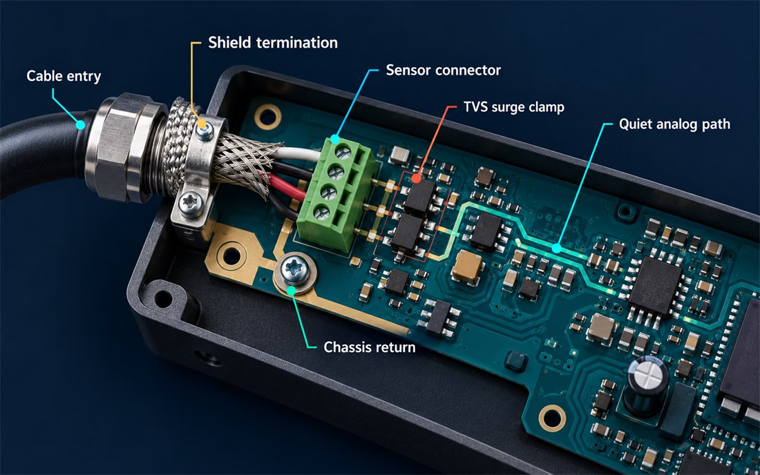
The conceptual illustration shows cable entry, shield termination, TVS placement, chassis return, and the quiet analog path. It is a design explanation, not a measured customer board. For a production IoT Sensor PCB, freeze the stackup and copper construction before the team tunes protection footprints; a plane split or via change can move the return current into the sensor area.
Separate shield, surge, and signal returns
Shield termination is a EMC containment review and a system decision. A 360-degree clamp at the enclosure entry can give high-frequency energy a short path, while a pigtail may add inductance that defeats the intended protection at fast edges. The choice for a IoT Sensor PCB depends on enclosure material, cable connector, safety requirements, and the allowed common-mode current. Document the mechanical contact and the PCB land pattern together so sensor connector inspection can cover both.
Place the first surge clamp close to the entry, before the line reaches the analog front end. Keep the protected trace short, avoid routing it parallel to a sensitive reference, and provide a defined return to chassis or the approved power return. A surge-current corridor is more useful than a vague “keep away” note because it gives layout and inspection teams a physical boundary.
The sensor signal still needs a quiet reference. A shield-to-chassis joint should not share a small solder neck with the ADC reference return. Separate the connector shield land, surge return, power return, and measurement return in the design review; then show where they join, if they must join, on the released drawing.
Protection parts also have tolerances and parasitics; include an inspection plan for the released footprint. Check their capacitance against the sensor bandwidth, leakage against the sleep current, and pulse rating against the installation environment. The approved alternate list should state which electrical parameters cannot change. Substituting a lower-capacitance part may preserve signal bandwidth but move surge energy into a regulator or processor pin.
Validate the interface as an assembly
A cable test that uses a loose clip is not a release method. Build a cable-fixture datum that controls connector seating, shield clamp pressure, cable bend, and chassis bonding. The fixture should expose approved test points without adding a long probe ground lead that changes the result. Record the sensor stimulus, supply state, firmware build, and enclosure condition for each run.
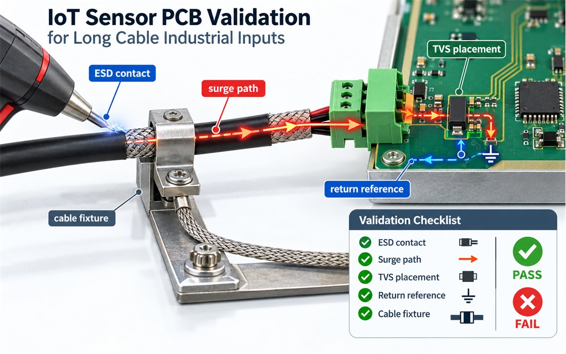
This second conceptual image separates ESD contact, surge path, return reference, TVS placement, and cable fixture checks. The pass/fail marks are a checklist illustration, not a test report. During a real review, use a return-path inspection to confirm copper, vias, solder fillets, and shield hardware before changing firmware thresholds.
Run the validation in layers. First verify continuity and polarity. Next exercise normal cable motion and connector insertion. Then apply the approved disturbance method while monitoring sensor validity, processor reset, supply recovery, and communication errors. A noise-observation point near the ADC reference and another at the connector return let the team distinguish conducted noise from a grounding mistake.
Release rules for industrial deployment
Project managers need a release package that survives supplier and enclosure changes. Include the cable specification, connector part number, shield termination detail, protection BOM, stackup, controlled impedance notes where applicable, fixture drawing, and acceptance criteria. A change-control matrix should identify which substitutions require a new disturbance check.
- Freeze connector pin order and the enclosure datum before panelization.
- Keep the shield and surge current path separate from the analog reference.
- Inspect TVS orientation, solder coverage, and chassis hardware on the first article.
- Repeat cable and ESD checks after coating, enclosure, or firmware changes.
- Log sensor lot, board revision, fixture revision, and cable length with every comparison.
An IoT Sensor PCB is ready for production when the board, cable, enclosure, and fixture produce the same electrical story. The value is not a single impressive bench trace; it is a repeatable interface that protects measurement integrity across installation, assembly, and controlled change.
Write a serviceable interface record
Service teams need more than a generic ESD statement. For an IoT Sensor PCB, the record should show the cable length class, shield termination, connector datum, TVS location, chassis bond, and approved return path. The IoT Sensor PCB revision should be tied to the fixture and firmware used during the last accepted disturbance check.
If an enclosure, cable supplier, or connector alternate changes, repeat the interface review before changing software thresholds. A second IoT Sensor PCB sample should be checked with the same cable fixture so the team can separate a board change from a setup change. The IoT Sensor PCB evidence makes a field decision faster and keeps a production deviation from becoming an undocumented redesign.
Sources: Analog Devices mixed-signal grounding and protection guidance; Würth Elektronik EMC and connector application notes; Qorvo RF and transient-control references; connector and sensor supplier technical data. Values above are engineering practices or design targets, not customer measurements.
