
Table of Contents
A battery-powered IoT Sensor PCB system uses an IoT Sensor PCB IoT Sensor PCB can miss its life target even when the firmware duty cycle looks efficient. The usual cause is not one large load; it is a repeated interaction between the sensor rail, regulator quiescent current, radio burst, leakage through protection parts, and a board return path that was never partitioned. A good design makes the energy path visible, gives the manufacturing team inspection points, and lets a project manager compare a prototype with the released assembly.
Why battery life is a PCB problem
The battery, connector, protection device, regulator, load switch, sensor, processor, and radio form one impedance network. A trace that is acceptable for average current may create a transient drop when the radio starts. The sensor may then take a sample while its supply is recovering, creating a false drift that software cannot reliably remove. A IoT Sensor PCB power review should list average current, peak current, wake interval, rail tolerance, and the state of every switched domain.
Begin with a power-tree review, not with a battery-life spreadsheet. Mark the battery entry, charger or protection, regulator, load switches, sensor rail, ADC reference, and radio burst path. The trace width, via count, connector contact, and plane transition then have a clear purpose. If a supplier substitutes a regulator or connector, the IoT Sensor PCB power tree must be reviewed again.
Partition sensor, processor, and radio rails
Place the sensor and its first decoupling close to the quiet rail. Keep the processor and radio burst currents from sharing the same narrow neck or via field. A sleep-domain split can reduce leakage, but only when the return path and enable logic are defined. Do not leave a disabled sensor powered through an I/O protection diode. Show the intended off-state on the schematic and the assembly drawing.
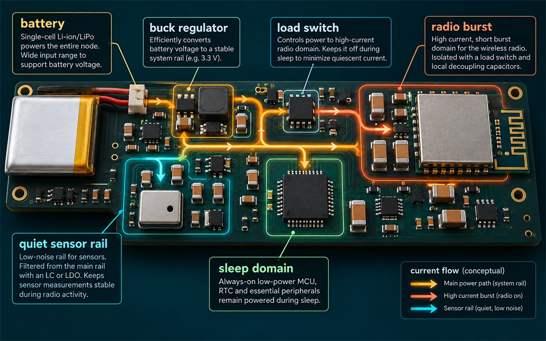
This conceptual figure shows a battery input, quiet sensor rail, load switch, sleep domain, and radio burst path. It is a design explanation, not a measured current trace. For a released IoT Sensor PCB, lock the laminate, copper, and plane construction before optimizing transient behavior. A change in stackup can change the loop area and thermal spreading that support the power path.
Place switches and capacitors where current actually flows
A load-switch placement should keep the switched node short and provide a direct return to the reservoir capacitor. The decoupling network needs values, voltage ratings, package sizes, and assembly access that are explicit. If a capacitor moves to the opposite side of the board, the electrical value may be unchanged while the loop inductance is not.
Make wake timing measurable
Low-power claims depend on timing. Define when the sensor powers, when it settles, when the ADC samples, and when the radio transmits. A wake-timing fixture should access approved test pads without forcing a long probe ground lead into the measurement. Provide a current-shunt or jumper location at the battery entry so average and peak behavior can be separated. The firmware build, sensor stimulus, supply voltage, and board temperature should be recorded with each comparison.
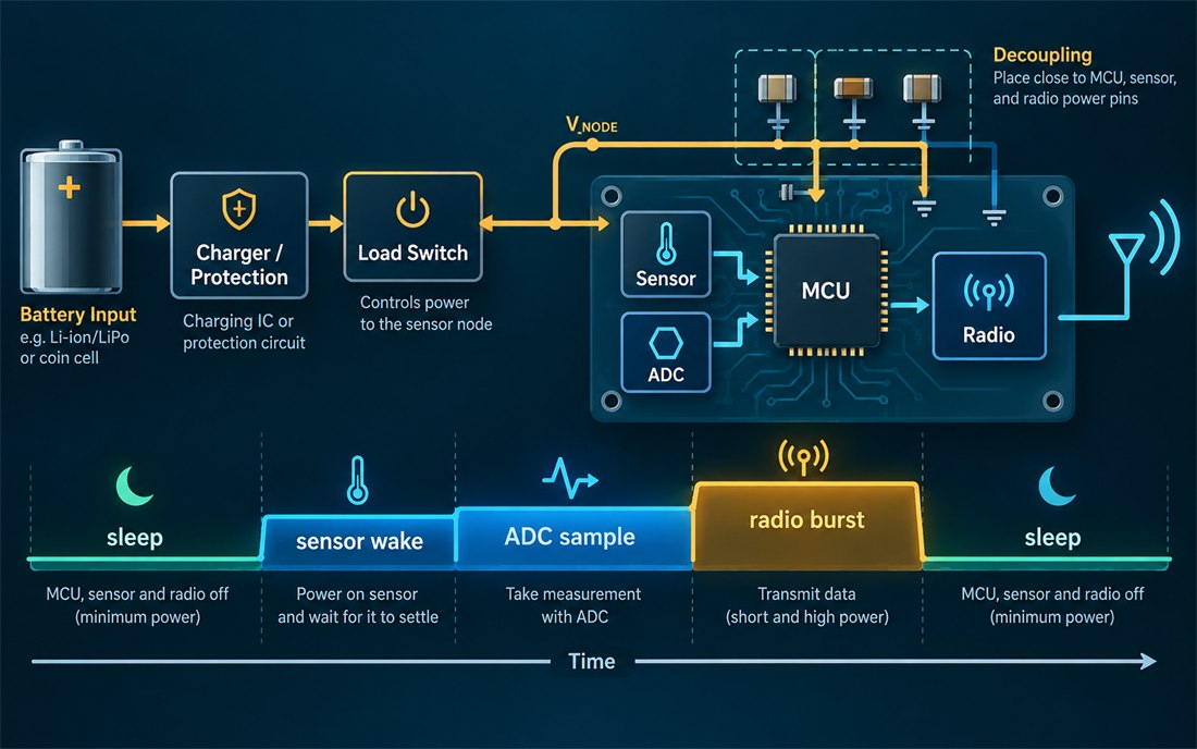
The second conceptual figure shows sleep, sensor wake, ADC sample, radio burst, and decoupling placement. It is not a customer waveform. Use the current-shunt access to identify whether a high reading comes from the radio, the regulator, leakage, or fixture loading. A power-path inspection should confirm the actual copper, vias, solder joints, and connector contacts before the team changes firmware limits.
Release power paths for assembly
Battery contacts and load switches are mechanical parts as well as electrical parts. Define the battery-connector seating, spring force, solder fillet, and fixture support. A shield or enclosure screw should not press on a switched node or crack a reservoir capacitor. The regulator’s thermal path should include copper area, via pattern, and assembly inspection.
Cleaning and coating can add leakage or change the sensor’s startup behavior. If the process changes, repeat the wake sequence after the approved dry and cure state. Record inrush limits and the protection device on the inrush-control note. A project team should distinguish a design target from a measured life result and avoid presenting one prototype battery test as a universal guarantee.
A production checklist for low-power nodes
- Freeze battery entry, protection, regulator, switched domains, sensor rail, ADC reference, and radio burst path.
- Show current loops, return vias, reservoir capacitors, test pads, and mechanical supports in controlled drawings.
- Define wake timing, current-shunt access, firmware build, stimulus, voltage, and temperature for comparisons.
- Inspect capacitor placement, switch orientation, via quality, battery contacts, and regulator thermal copper.
- Repeat the energy and sensor-settling review after component, coating, cleaning, or enclosure changes.
- Route any firmware or hardware substitution through a firmware-hardware change review.
A well-partitioned IoT Sensor PCB gives the product team a repeatable energy path instead of a battery-life number tied to one bench setup. The objective is to make current loops, timing, assembly state, and change control visible enough to support a reliable production decision.
Use an evidence-based handoff
The handoff should carry more than a schematic and a nominal battery capacity. Attach the rail map, sleep-state definition, connector drawing, approved component alternates, and inspection points that distinguish a normal wake cycle from a fault. For an IoT Sensor PCB, record the firmware build, regulator lot, sensor lot, battery source, and board revision beside each power observation. This makes a range complaint traceable instead of turning it into a debate between software and hardware teams.
Before volume release, ask manufacturing to demonstrate probe access, polarity control, connector seating, and rework limits on a representative panel. Ask the project manager to freeze the power-tree assumptions in the change log. If the radio, enclosure, battery, or sensor changes later, the same checklist can be rerun without rebuilding the measurement method from memory.
Sources: Analog Devices power and mixed-signal layout guidance; Würth Elektronik power integrity and assembly notes; Qorvo RF burst integration guidance; laminate and connector supplier technical data. Values above are engineering practices or design targets, not customer measurements.
