
Table of Contents
A LoRa PCB can pass schematic review and an antenna tuning check, then lose range after the array is depanelized. The failure on a LoRa PCB is rarely mysterious: the board edge, tooling holes, V-score, mouse-bites, connector body, and antenna keep-out were treated as mechanical details instead of RF datums. When a panel is routed, snapped, or milled, local stress can move the relationship between the antenna, ground boundary, and enclosure wall. A project team then spends days retuning a board that was never dimensionally released.
Why a sound RF layout can shift at depanelization
At sub-GHz frequencies the wavelength is long, but the antenna still depends on its immediate copper and mechanical environment. A ground pour that ends a few millimetres from the radiator, a shield edge that moves toward the feed, or a connector that tilts under panel stress can change the launch condition. The relevant question is not whether the finished board is electrically continuous; it is whether the RF datum remains in the same position from panel fabrication to enclosure assembly.
Use the antenna keep-out review to identify every feature that can become a clamp, breakaway tab, or routing reference. A keep-out should include the radiator, its return-current corridor, and the enclosure wall that will be used during final tuning. Record the mechanical origin in the drawing, not only in the CAD file. That allows a LoRa PCB review to compare the RF geometry with the panel tooling plan.
Choose a panel edge that protects the antenna datum
Panelization is a compromise between throughput and local board integrity. A routed outline gives a clean edge but consumes rail width; a V-score is efficient for rectangular boards but can leave a residual ridge; mouse-bites improve nesting but introduce concentrated fracture points. None is automatically correct for a radio board. Keep breakaway features away from the antenna feed and from any long edge that acts as a counterpoise. If the antenna must sit near an edge, place the breakaway pattern on the opposite side and show the restricted zone on the fabrication drawing.
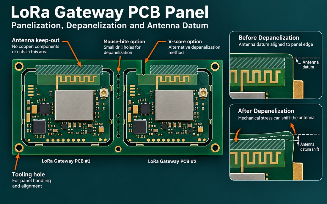
The illustration shows a conceptual LoRa PCB panelization review, not a measured customer board. In a real release, the team should compare the panel rail, the finished outline, and the antenna datum in one controlled drawing. A practical RF ground-return plan also reserves a continuous path under the feed so a small edge burr or copper pullback does not create an unintended discontinuity.
Do not let the tooling plan become an RF change
Tooling holes and fiducials should be outside the RF exclusion zone, but they still influence how the panel is supported. If a fixture clamps on an antenna edge, board flex can appear as a tuning shift. Place support points under mechanically stiff regions and communicate the support map to the assembler. The tooling-hole datum should reference the finished board origin, while the panel drawing records the rail origin. This distinction prevents a panel supplier from silently relocating the antenna relative to the enclosure.
How a LoRa PCB Carries Holes, Rails, and Connector Loads
A coax or board-edge connector can turn a small mechanical error into a field failure. The connector body may pull the board toward a metal wall, and a screw or spring contact can push against the opposite edge. Define the connector launch as a mechanical and RF feature: include the mounting keep-out, the return-via pattern, and the datum used by the enclosure drawing. When a test cable is attached, the load should be carried by the fixture or chassis, not by the antenna substrate.
For high-volume builds, specify the edge-plating and profile check that protects exposed contacts and keeps burrs away from the RF boundary. A controlled assembly fixture should support the board at repeatable points during connector insertion and soldering. If the fixture changes between prototype and production, repeat the mechanical datum review before approving a new range target.
Make mechanical release part of RF verification
RF verification should start with a visual and dimensional gate. Confirm the finished outline, antenna-to-edge distance, connector height, hole position, and copper clearance against the released drawing. Then inspect the ground return and feed transition. A mechanical drawing review and an first-article inspection are not substitutes for RF testing; they are the controls that make an RF comparison meaningful.
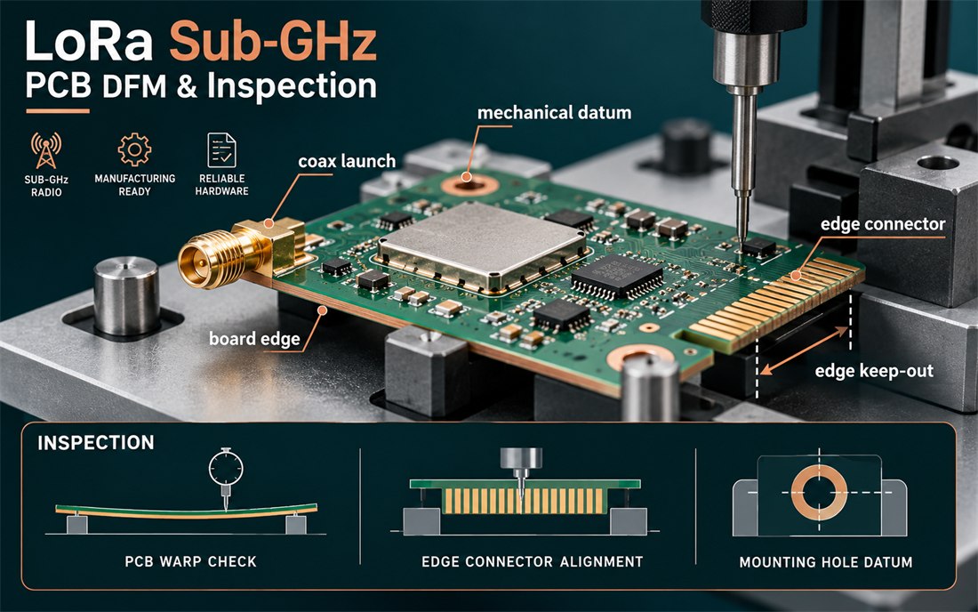
The second illustration represents a conceptual fixture and datum inspection. It should not be described as a measured result. During a release, capture the board orientation, fixture contact points, cable routing, and enclosure state. The depanelization control should record whether the board was routed, scored, or broken, because those methods create different edge conditions. Keep a test-fixture record with the lot traveler so an unexpected sensitivity change can be traced to handling rather than blamed on the laminate.
Release a LoRa PCB with a stable mechanical datum
When a prototype is tuned on a bench, the cable, clamp, and operator hand can accidentally become part of the antenna system. A production release should therefore separate three records: the dimensional record, the assembly record, and the RF comparison record. The dimensional record confirms the finished outline, edge condition, hole position, and connector seating. The assembly record identifies the stencil, fixture support points, cleaning state, and any approved rework. The RF record then states which enclosure, cable orientation, and board support were used. This separation helps a project manager decide whether a range change is a design issue or a process change.
For a LoRa PCB, keep the release package under revision control. If the panel rail width, depanelization tool, connector supplier, or enclosure fastener changes, route the change through the same review. A controlled return-path inspection should confirm that the new mechanical feature has not cut across the intended current corridor. The final traveler should name the LoRa PCB revision and its mechanical datum. The goal is not to promise identical field performance without testing; it is to make every comparison repeatable enough that the next engineering decision is based on evidence.
A release checklist for production
- Freeze the antenna, ground boundary, enclosure wall, and connector datum in one drawing.
- Mark the antenna keep-out on the panel drawing and prohibit breakaway features inside it.
- Separate panel and finished-board origins; dimension tooling holes from the correct datum.
- Define profile, burr, edge copper, and connector seating checks for first article and lot inspection.
- Use the same support and cable-loading condition for prototype comparison and production verification.
- Record the depanelization method, fixture ID, and enclosure state with any range or sensitivity result.
A disciplined release lets a LoRa PCB move from panel to enclosure without turning a mechanical operation into an RF redesign. For a LoRa PCB, the engineering payoff is not a promised range number; it is a stable datum, a traceable inspection record, and a production decision that can be repeated.
Sources: Taconic RF laminate technical data and application guidance; Würth Elektronik RF layout and connector application notes; Analog Devices RF grounding and mixed-signal layout guidance; Qorvo front-end and antenna integration documentation. Values in this article are engineering practices and design targets, not customer measurements.
