
Table of Contents
A remote node built around a LoRa PCB may pass a bench range check and then miss packets when its own transmitter, sensor heater, or regulator changes state. The failure is often blamed on the radio firmware, but the board can be the coupling path: a switching node injects energy into the receiver rail, a shared return moves the reference of the low-noise amplifier, or a shield can lands on a noisy copper island. A LoRa PCB should therefore be reviewed as a power-distribution system as well as an RF carrier.
Why a quiet receiver can fail under transmit load
For a LoRa PCB, the most useful observation is the timing of the failure. If packet loss appears only while the power amplifier transmits, during sensor warm-up, or when a cellular modem wakes, the first question is whether the receiver rail and its return path remain quiet. A LoRa PCB can show a large range difference without any change to the antenna when a regulator inductor, shield, or cable shares the same current loop as the RF module.
Separate conducted sensitivity from radiated behavior. A conducted check can isolate the radio and matching network, while a system check includes the enclosure, cable, battery impedance, and digital traffic. Use the same supply harness and operating state for both. This prevents a project team from changing the antenna to compensate for a rail disturbance that originates in the power tree.
For a remote sensor product, define a quiet-state and a worst-case-state test. The worst case should include the highest expected processor activity, the transmitter duty cycle, sensor excitation, and any boost or buck transitions. A mixed-signal PCB design review can then map which current loops are allowed to cross the RF boundary and which must remain local to the converter.
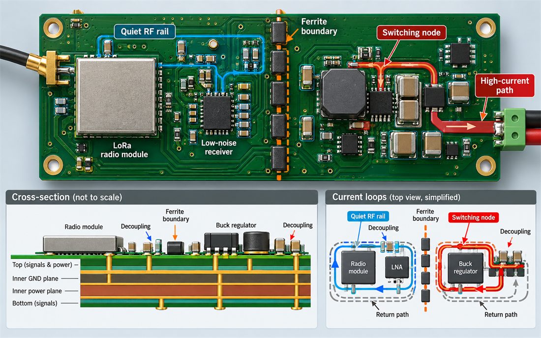
Partition the power path before routing
Keep the switching loop physically small
Place the regulator, inductor, catch diode or synchronous FETs, and input/output capacitors as one compact loop. Route the high di/dt path on the layer with the shortest return. A LoRa PCB with a long switch-node trace can radiate into the RF module even when the trace is far from the antenna. Keep copper under the switch node intentional; a void that is not documented can create an unpredictable field and return path.
Use a ferrite, filter, or load-switch boundary only when the impedance and current rating match the operating mode. The filter is not a substitute for placement. Its input and output returns must not share the same narrow neck with the receiver reference. A clear LoRa PCB drawing should identify the quiet rail, the high-current rail, and the point where they join.
Make the receiver reference plane continuous
Keep the receiver, matching network, crystal, and low-noise supply over a continuous reference plane. Avoid routing a sensor clock, display interface, or motor control line through the return path underneath the radio. If a split is unavoidable, bridge it at a controlled datum rather than allowing current to choose a path around a mounting hole or connector.
Decoupling works when the capacitor, via pair, and load pin form a short loop. Document the intended capacitor case size and placement side. A stackup release should keep the power and ground layers at a repeatable distance so that the same capacitor placement has a similar loop inductance from lot to lot.
Keep decoupling and shielding stable through assembly
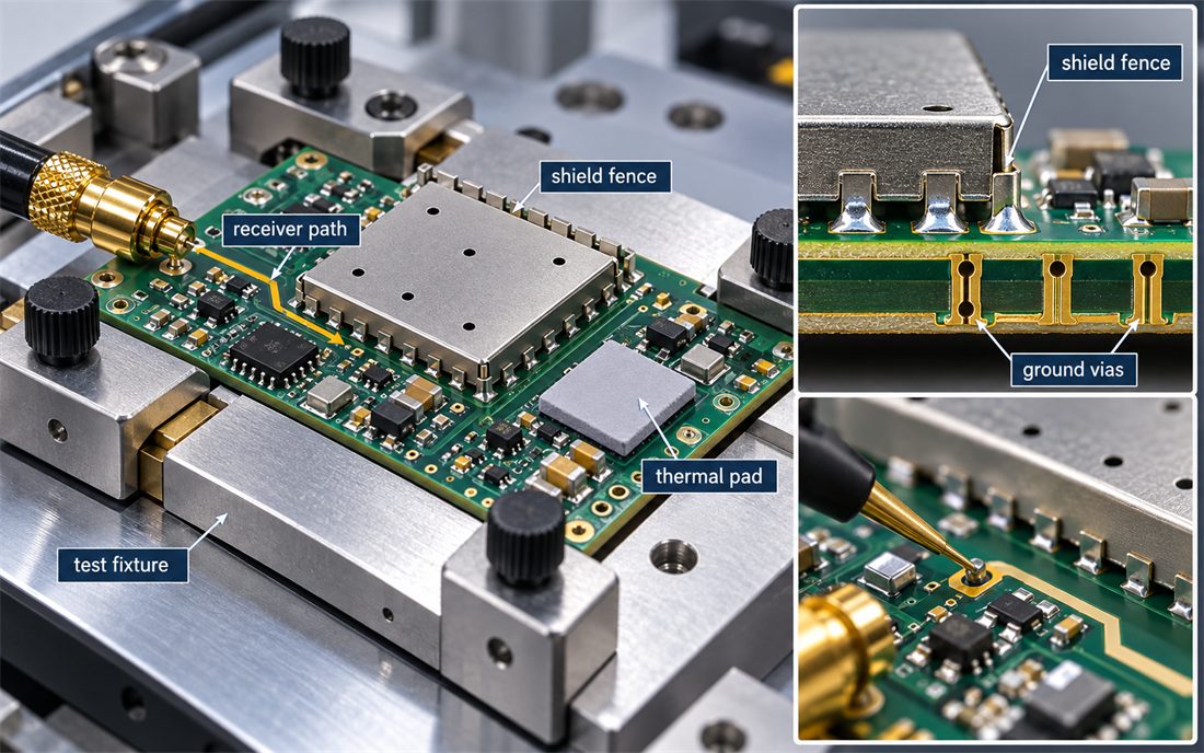
On a LoRa PCB, power-integrity failures are often introduced during assembly rather than schematic design. A shifted 0402 capacitor, a tombstoned ferrite, or an incomplete shield solder joint changes the local current loop. Put the radio module, decoupling array, and shield fence on the same first-article inspection view. A PCB assembly drawing should call out polarity, exposed-pad solder coverage, and the no-clean or cleaning route around the RF module.
Shield cans need a defined landing pattern and a controlled ground-via fence. Do not let a keep-out for the can opening interrupt the receiver return. If a thermal pad uses a large paste window, review whether the reflow profile can pull the module or create voids that change its ground contact. Use a shield-fence inspection point in the first article instead of relying on a visual check from one angle.
A production LoRa PCB fixture can also change the result. Spring probes, clamps, and battery simulators should contact the same datum on every unit. A test fixture that presses near the module can flex the board and change a marginal solder joint. Define probe force, support points, cable routing, and the order of radio, sensor, and power tests.
Release power integrity as a production characteristic
A repeatable release package connects the power-tree review to the RF acceptance plan. Include converter part numbers, inductor saturation assumptions, capacitor dielectric and case size, filter placement, layer references, and the defined radio test state. The laminate and copper specification should match the released stackup rather than a generic board note.
At first article, inspect the switch-node geometry, decoupling placement, shield solder, via fence, and ground continuity. A via and plating check is useful where the receiver reference depends on multiple ground transitions. During functional test, log the supply mode, battery or bench source impedance, transmitter state, and firmware build. This makes a sensitivity change traceable to a board, process, or configuration.
If a component is substituted, compare its impedance, package parasitics, current rating, and thermal behavior; “same value” is not RF equivalence. A LoRa PCB should identify whether the substitution changes the quiet rail, switch-node boundary, or shield landing. If it does, repeat the relevant power and conducted-RF checks before releasing the next panel.
Keep the final evidence concise: a controlled stackup, annotated power tree, first-article photographs, fixture setup, and a comparison table for quiet and worst-case modes. A DFM handoff can then translate the RF intent into drill, copper, mask, assembly, and inspection instructions. The goal is not to promise a universal noise number; it is to ensure that every KKPCB production release preserves the same current loops that were approved during design.
Sources: Semtech LoRa radio application guidance, regulator and ferrite manufacturer data sheets, IPC assembly and solder-joint guidance, and KKPCB internal RF/power-integrity release practices were used as engineering references. Values described here are design targets or process controls, not customer measurement claims.
