
Volume release exposes the difference between a ceramic layout and a ceramic process. Screen, thick-film, thin-film, plated, brazed, and bonded features each have a different capability window. An Alumina PCB drawing that specifies only line widths and hole sizes can still leave the supplier guessing about paste, firing, edge handling, carrier support, and inspection. The project needs a DFM package that is specific enough to quote and flexible enough to control approved changes.
Call out the metallization process
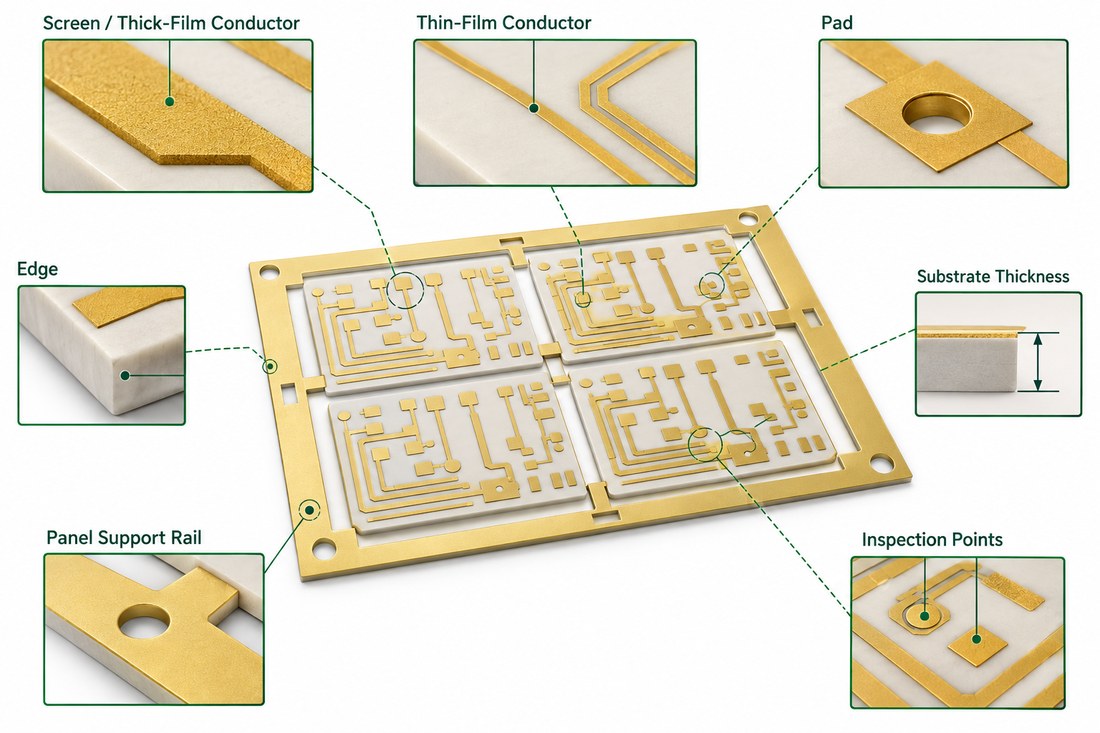
List the conductor system, thickness or resistance target, adhesion requirement, pad finish, and any wire-bond or solder interface. The Alumina PCB material and metallization callout should identify the supplier data sheet revision and the allowed alternate process.
The RF PCB manufacturing review should mark critical line width, spacing, pad flatness, vias, cavities, and edge features. A generic PCB rule table is not a substitute for the ceramic process capability.
Add panel handling requirements where the substrate is thin, large, or populated with heavy copper. Show support rails, protective film, breakaway method, and the inspection access that must remain open.
Make inspection reflect the product feature
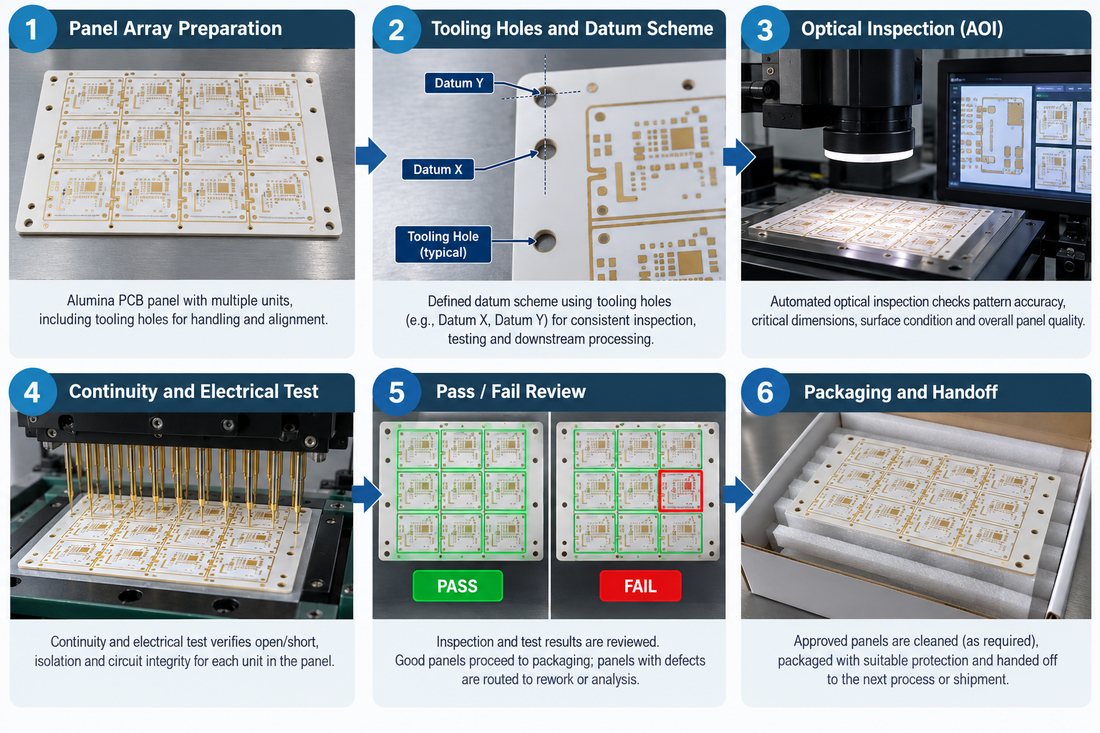
Plan cross-sections, continuity checks, visual standards, dimensional inspection, and any bond or solder evidence before the first lot. The Alumina PCB acceptance plan should identify which feature is sampled, how it is measured, and which lot it represents.
A witness coupon is valuable only when it shares the metallization route and thermal history of the product. The controlled impedance quality package should state the relationship between the coupon and the actual RF, power, or sensor feature.
Keep critical datums consistent from artwork to panel to inspection report. A shifted coordinate system can make a compliant feature appear out of tolerance or hide an edge defect.
Protect procurement and ECO control
Ceramic material, conductor paste, firing profile, and surface finish must remain synchronized in the purchase order and drawing. The thermal management procurement note should require engineering approval for any substitute that changes dielectric, thermal, CTE, or metallization behavior.
When an ECO changes a pad, edge, cavity, or copper density, review panel handling and inspection access again. A layout-only ECO is not safe when it changes process stress or measurement location.
Use a final release checklist: material revision, metallization, panel, datums, inspection plan, packaging, approved alternates, and deviation owner. This is the minimum information needed to move from prototype confidence to a repeatable lot.
Alumina PCB DFM succeeds when the ceramic process is written into the release. Make metallization, handling, inspection, and substitutions explicit before the volume purchase order.
Implementation note for this DFM, metallization, and volume release review: keep the engineering assumption visible at the point where it affects a drawing, a supplier quote, or an inspection record. Ask the design owner to identify the reference plane, interface datum, and acceptance method before the release is frozen. Ask manufacturing to return the proposed stack, panel, and process window rather than a generic capability statement. Ask assembly to identify the profile, cleaning, and support conditions that could move the RF or thermal result. This simple handoff prevents a typical material value from being mistaken for a guaranteed product result and gives the project team a clear action when an ECO changes the physical boundary.
Release note: keep the Alumina PCB metallization, panel handling, and inspection evidence under one revision before volume release.
Sources: Panasonic MEGTRON technical material guidance; Rogers and Taconic high-frequency material data sheets where relevant; CeramTec ceramic substrate data; Analog Devices RF and mixed-signal layout guidance. Numerical values are treated as typical supplier values or engineering targets unless the released drawing defines a measured acceptance value.
Release note: confirm the Alumina PCB construction before the next ECO.
Release note: confirm the Alumina PCB construction before the next ECO.
Release note: confirm the Alumina PCB construction before the next ECO.
Release note: confirm the PCB manufacturing evidence before approval.
Release note: confirm the PCB assembly evidence before approval.
