
A high-power Alumina PCB can carry heat efficiently only when the copper, substrate, solder or braze, and metal carrier move together. Repeated temperature change makes the interface a mechanical system. The most common project mistake is to qualify the ceramic coupon while the product uses a different copper area, fastener pattern, or thermal interface. A reliable design begins by matching the test article to the production boundary.
Map the stress before adding copper
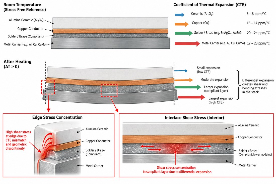
Large copper spreads heat but also creates local stiffness and CTE mismatch. The Alumina PCB floorplan should identify copper islands, carrier interfaces, solder or braze regions, and the neutral axis. Use fillets, slots, or compliant layers deliberately rather than as cosmetic fixes.
The RF PCB thermal review should list the substrate grade, copper thickness, interface material, and mounting condition. Supplier thermal conductivity is a typical material value; the assembly thermal resistance depends on contact, voids, flatness, and airflow.
Keep high-current paths broad through the power region but preserve the RF or sensor return path. A thermal copper change should trigger an electrical review if it changes the reference plane or the connector launch.
Design the cycle and inspection together
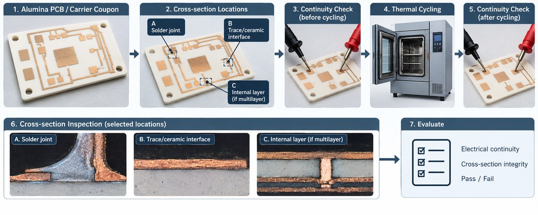
Define the thermal-cycle range, dwell, ramp, sample configuration, and failure criteria before the first qualification run. The Alumina PCB product should be represented with its actual carrier, fasteners, and interface material, not only a small material coupon.
The controlled impedance manufacturing plan should identify cross-section locations, void inspection, copper adhesion evidence, and any electrical continuity check after cycling. A passed cycle is meaningful only when the sample identity and fixture are recorded.
If a crack, delamination, or lifted interface is observed, classify the location and mechanism before changing the drawing. Replacing a copper thickness without understanding the stress path can move the problem rather than solve it.
Release changes with a thermal risk matrix
When a device, carrier, or fastener changes, update the thermal and mechanical risk matrix. The thermal management project record should state whether the change affects heat flow, stress, RF return, or inspection access.
Keep a defined range for flatness and mounting pressure. Over-constraining a ceramic board can be as risky as leaving it unsupported.
Close the release with the material revision, copper map, interface note, cycle plan, and deviation owner. This gives quality and procurement a common basis for approving the next lot.
Alumina PCB high-power reliability is an interface problem. Control copper geometry, mounting compliance, thermal-cycle evidence, and change triggers as one release package.
Implementation note for this high-power thermal cycling review: keep the engineering assumption visible at the point where it affects a drawing, a supplier quote, or an inspection record. Ask the design owner to identify the reference plane, interface datum, and acceptance method before the release is frozen. Ask manufacturing to return the proposed stack, panel, and process window rather than a generic capability statement. Ask assembly to identify the profile, cleaning, and support conditions that could move the RF or thermal result. This simple handoff prevents a typical material value from being mistaken for a guaranteed product result and gives the project team a clear action when an ECO changes the physical boundary.
Release note: keep the Alumina PCB thermal-cycle assumptions tied to copper geometry and interface materials so a reliability result remains meaningful after an ECO.
Sources: Panasonic MEGTRON technical material guidance; Rogers and Taconic high-frequency material data sheets where relevant; CeramTec ceramic substrate data; Analog Devices RF and mixed-signal layout guidance. Numerical values are treated as typical supplier values or engineering targets unless the released drawing defines a measured acceptance value.
Release note: confirm the Alumina PCB construction before the next ECO.
Release note: confirm the Alumina PCB construction before the next ECO.
Release note: confirm the Alumina PCB construction before the next ECO.
Release note: confirm the PCB manufacturing evidence before approval.
Release note: confirm the PCB assembly evidence before approval.
