
At mmWave frequencies, the cavity, copper edge, connector launch, and antenna clearance become part of the circuit. A Ceramic PCB is often selected for its dimensional stability and integration potential, yet a cavity that is only slightly too deep or a ground fence that is interrupted by a tooling keep-out can move the resonance enough to invalidate the first prototype. The most expensive project failures are not caused by one wrong trace width. They come from releasing a mechanical drawing, RF layout, and ceramic process as if they were independent documents.
Table of Contents
- Freeze the electromagnetic boundary
- Build the feed and return together
- Prevent enclosure changes from becoming RF changes
Freeze the electromagnetic boundary
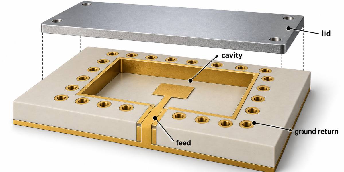
Begin with a boundary drawing that identifies the radiating region, the cavity wall, the reference conductor, and every metal feature within the near field. The Ceramic PCB should have a named datum for the antenna edge and a separate datum for the connector or feed. This avoids dimension chains that accumulate through a carrier, lid, or machined pocket.
Use the supplier process capability to choose the cavity tolerance, metallization thickness, and corner radius. Do not copy a generic ceramic tolerance into a mmWave design. The released drawing should distinguish a design target from a guaranteed process limit and should name the inspection method for the critical depth and step.
The RF PCB review should include the antenna simulator assumptions, but the production drawing must remain readable to the fabricator. Mark keep-outs as geometry, not prose, and call out any area where a mounting screw, shield, or adhesive is allowed to enter the RF boundary.
Build the feed and return together
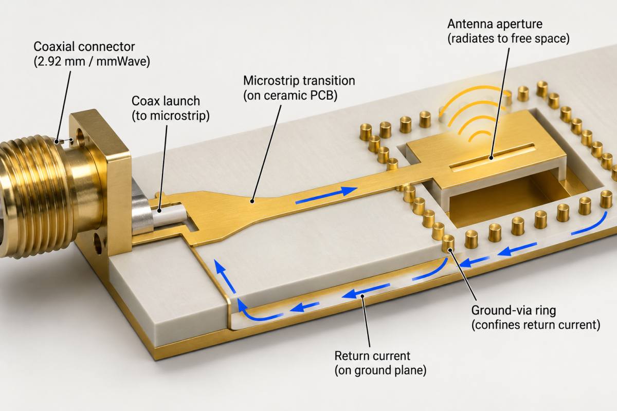
A feed transition can look correct in a top view while the return path is broken in the third dimension. Place ground vias or metallized sidewalls close to the feed and show the intended current loop across the cavity. Analog Devices guidance recommends minimizing via inductance and keeping the return path continuous when a signal changes layers; adapt that principle to the ceramic via technology actually quoted.
For a coax or waveguide launch, align the connector pin, pad, cavity edge, and first ground feature to one datum system. The controlled impedance layout page should show the launch section as a controlled region with no unrelated copper pours. If the launch uses a stepped pad, document the step and the inspection access before sending the design to panelization.
Treat the first prototype as a geometry correlation build. The goal is to compare the released dimensions, the fabricated cross-section, and the RF response under a defined fixture. Do not label a curve as measured unless the project records the fixture, calibration, and sample identity.
Prevent enclosure changes from becoming RF changes
A lid or gasket can detune a cavity when its spacing, plating, or compression changes. Add the enclosure interface to the design review and set a change trigger for any metal or dielectric part within the antenna keep-out. The Ceramic PCB should not be approved by the PCB team alone when the cavity is part of the antenna.
For manufacturability, allow a clear inspection route for cavity depth, sidewall metallization, and connector coplanarity. Ask the thermal management partner to return a process drawing with datums, tooling zones, and the proposed coupon locations. A short DFM loop at this stage is faster than changing the cavity after the first RF build.
Release the package with a geometry checklist: antenna datum, feed datum, cavity depth target, wall continuity, ground return, enclosure clearance, and the exact revision of the material data sheet. That checklist gives the project manager a concrete gate before procurement.
A mmWave Ceramic PCB succeeds when the electromagnetic boundary and the manufacturing boundary are the same drawing. Make the cavity, feed, return, and enclosure interfaces explicit, then verify the fabricated geometry before interpreting RF data.
Implementation note for this mmWave cavity and antenna co-design review: keep the engineering assumption visible at the point where it affects a drawing, a supplier quote, or an inspection record. Ask the design owner to identify the reference plane, interface datum, and acceptance method before the release is frozen. Ask manufacturing to return the proposed stack, panel, and process window rather than a generic capability statement. Ask assembly to identify the profile, cleaning, and support conditions that could move the RF or thermal result. This simple handoff prevents a typical material value from being mistaken for a guaranteed product result and gives the project team a clear action when an ECO changes the physical boundary.
For this mmWave Ceramic PCB, freeze the cavity and feed datums together; a geometry change that looks mechanical can still alter the antenna boundary and the launch correlation.
The Ceramic PCB antenna cavity should be frozen with the feed, ground wall, and enclosure datum so the first RF build has a repeatable geometry.
A second Ceramic PCB antenna cavity review should compare the released geometry with the fabricated cavity and connector datum before RF tuning.
The Ceramic PCB antenna cavity release should retain the connector revision and cavity inspection record beside the RF data.
Sources: Panasonic MEGTRON technical material guidance; Rogers and Taconic high-frequency material data sheets where relevant; CeramTec ceramic substrate data; Analog Devices RF and mixed-signal layout guidance. Numerical values are treated as typical supplier values or engineering targets unless the released drawing defines a measured acceptance value.
Release note: confirm the Ceramic PCB construction before the next ECO.
Release note: confirm the Ceramic PCB construction before the next ECO.
Release note: confirm the PCB manufacturing evidence before approval.
Release note: confirm the PCB assembly evidence before approval.
