
A high-power RF module can meet its electrical target and still fail in the field because the heat path was never released as a complete system. A Ceramic PCB changes the design conversation: the ceramic substrate, copper pattern, attach method, via or metallized interface, and the enclosure all share the same thermal boundary. The project pain usually appears late, when a copper land is flat enough for RF assembly but not flat enough for the required interface pressure, or when a nominal thermal value is treated as a guaranteed junction temperature. This article gives engineers and project managers a way to freeze the thermal interface before fabrication.
Table of Contents
- Start with the heat path, not the material name
- Coordinate RF return current with the thermal copper
- Assembly and release controls
Start with the heat path, not the material name
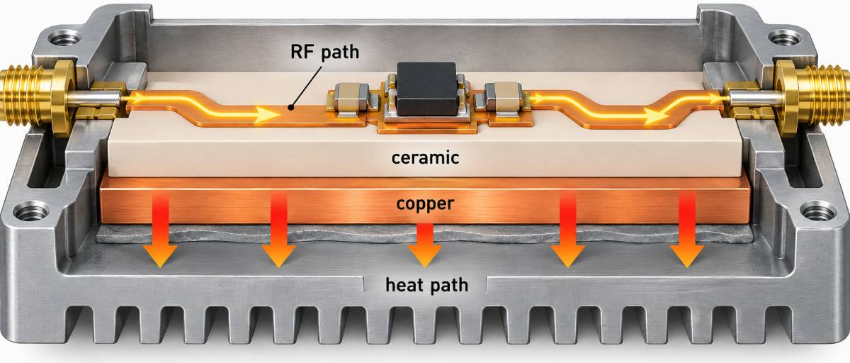
Map the path from the active device to the enclosure: die attach or exposed pad, top copper, ceramic, backside metallization, interface material, and chassis. A Ceramic PCB is valuable when the path is short and stable, but its benefit is lost if the mounting surface introduces a thick void-prone interface. Use a thermal resistance budget as a design target, then document which terms are supplier typical values and which terms must be verified on the released assembly.
For RF power amplifiers, copper thickness and copper spread can dominate the local temperature gradient. Keep the RF launch and the thermal spreader in the same coordinate system so a late pad change does not move the return path. If the board uses a copper slug or a metal carrier, define the mating flatness, surface finish, and screw or clamp load in the mechanical drawing rather than leaving them to assembly interpretation.
A useful early review links the RF PCB drawing to the device land pattern. The drawing should show the thermal pad, nearby ground stitching, keep-outs for solder fillets, and the measurement location that will be used during qualification. Avoid claiming a measured temperature until the exact device, fixture, airflow, and power profile are known.
Coordinate RF return current with the thermal copper
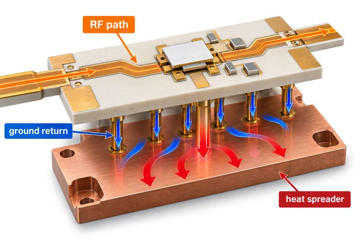
Thermal copper is not automatically a good RF reference. Large copper areas can interrupt a controlled transmission line when clearances or slots are introduced for mechanical reasons. Keep a continuous return plane under the signal path, then use a deliberate transition into the high-current thermal region. The Ceramic PCB layout should show where RF ground vias, thermal vias, and mounting vias may share or must separate barrels.
At a connector or package edge, place the RF launch first and then surround it with a repeatable ground-via pattern. Analog Devices layout guidance emphasizes a low-inductance return path and nearby stitching when a signal changes layers. Treat that as a layout rule to validate against the actual ceramic process, not as a substitute for a field solver.
When the thermal spreader crosses a split or carrier seam, review the current return in three dimensions. A short simulation or coupon can be a design target, but the production release still needs pad dimensions, drill tolerances, and inspection points that the fabricator can measure.
Assembly and release controls
Ceramic surfaces are less forgiving of uneven paste, excessive bending, and uncontrolled rework. Define stencil aperture reductions, placement force, reflow profile window, and cleaning limits with the assembler. The controlled impedance handoff should identify whether the exposed pad is soldered, sintered, brazed, or mechanically clamped; each option changes voiding risk and rework strategy.
For a first build, request a panel drawing that keeps the thermal reference coupon and the RF coupon in the same process family. The thermal management package should include the ceramic thickness, copper adhesion system, surface finish, and the acceptable bow or twist. If the ceramic is supplied as a carrier-mounted part, state which dimensions belong to the carrier and which belong to the finished board.
Before volume release, use a cross-functional checklist: RF path and thermal path reviewed together, interface pressure defined, supplier typical values separated from acceptance criteria, and a change-control owner named. This protects the project schedule when the device vendor changes the exposed pad or the enclosure design moves a fastener.
The practical decision is not simply whether a Ceramic PCB conducts heat. It is whether the released stack, copper interface, mounting method, and RF return can be built and inspected as one controlled assembly. Freeze those interfaces early and the thermal margin becomes a managed engineering variable instead of a late-stage surprise.
Implementation note for this thermal interface and power RF review: keep the engineering assumption visible at the point where it affects a drawing, a supplier quote, or an inspection record. Ask the design owner to identify the reference plane, interface datum, and acceptance method before the release is frozen. Ask manufacturing to return the proposed stack, panel, and process window rather than a generic capability statement. Ask assembly to identify the profile, cleaning, and support conditions that could move the RF or thermal result. This simple handoff prevents a typical material value from being mistaken for a guaranteed product result and gives the project team a clear action when an ECO changes the physical boundary.
For this Ceramic PCB power interface, keep the thermal datum, RF return, and assembly acceptance note in the same release package so a copper or carrier change can be reviewed without reopening the entire board.
The Ceramic PCB thermal interface is the boundary that ties the RF return, thermal spreader, and mounting method to one acceptance plan.
Sources: Panasonic MEGTRON technical material guidance; Rogers and Taconic high-frequency material data sheets where relevant; CeramTec ceramic substrate data; Analog Devices RF and mixed-signal layout guidance. Numerical values are treated as typical supplier values or engineering targets unless the released drawing defines a measured acceptance value.
Release note: confirm the Ceramic PCB construction before the next ECO.
Release note: confirm the Ceramic PCB construction before the next ECO.
Release note: confirm the PCB manufacturing evidence before approval.
Release note: confirm the PCB assembly evidence before approval.
