
A Megtron 7 PCB stackup must be frozen as an electrical and manufacturing contract before layer count or impedance changes are approved.
High-layer-count digital boards rarely fail because an engineer forgot to draw a trace. They fail when a late layer move changes dielectric thickness, resin distribution, or reference-plane continuity and the impedance model is not rebuilt. A well-controlled Megtron 7 PCB is only the starting point; the stackup must be frozen as an electrical and manufacturing contract.
Define the stackup architecture
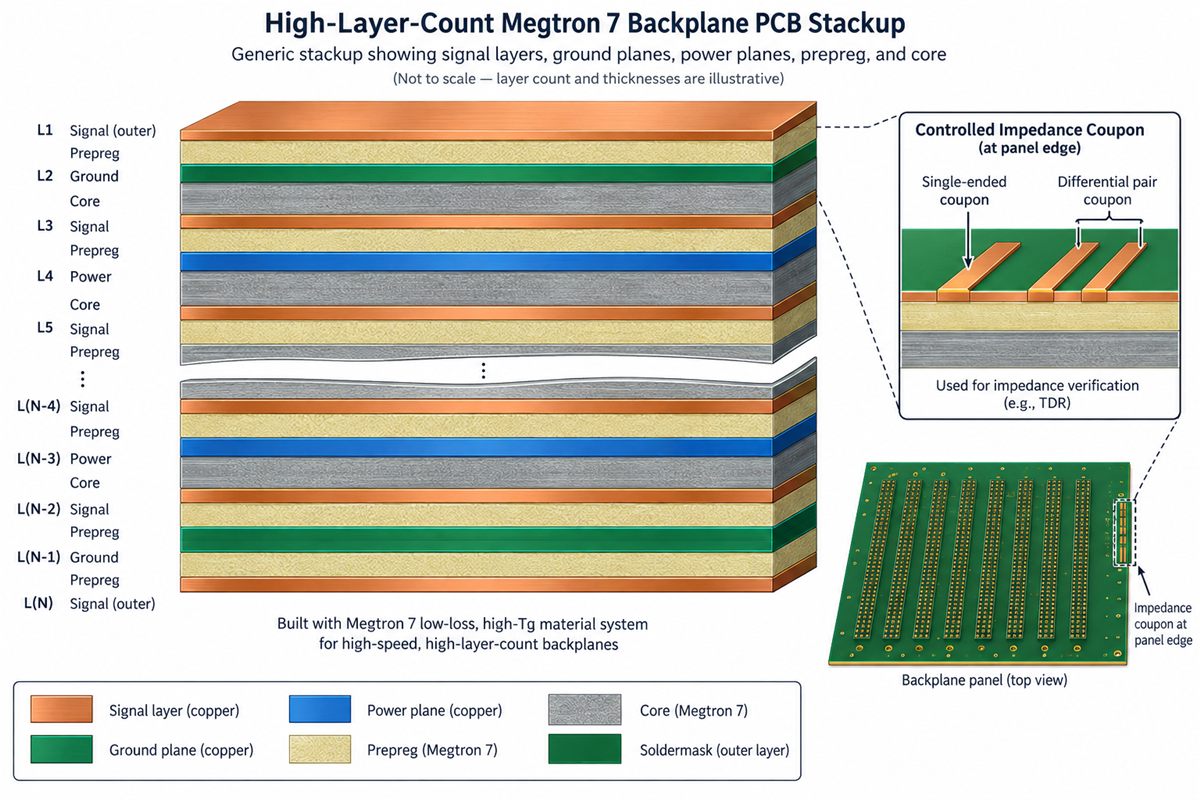
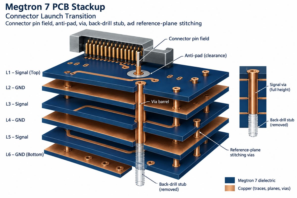
Start by classifying layers as stripline, microstrip, power, or low-speed utility. Every high-speed layer needs a continuous reference plane and a documented return-current path. Keep adjacent signal layers from sharing an ambiguous reference when a connector or via field forces a transition. The core/prepreg combination should be selected with the finished dielectric thickness in mind, not only the nominal supplier thickness.
Panasonic describes MEGTRON 7 as compatible with high-layer-count and large-format layouts. Its published typical data show Tg near 200 °C and low Dk/Df values that vary by grade, glass cloth, and test frequency. Use those numbers as inputs to the field solver, then replace the nominal dielectric with the fabricator’s controlled finished thickness range. A controlled-impedance PCB design review should record target impedance, tolerance, copper thickness after plating, and the reference plane used for each route.
Plan resin and press behavior
Resin content is not a cosmetic detail. It changes the effective dielectric constant and the final gap between copper and plane after lamination. Two layers with the same nominal thickness can produce different impedance if their glass style and resin percentage differ. Do not average the entire board: identify the specific prepreg pair around each critical line and ask the fabricator for a press thickness range.
Large boards also need copper-balance planning. A dense connector region beside a sparse power area can produce local press variation, registration drift, or bow and twist. Add copper thieving where it does not disturb controlled fields, keep plane openings symmetric, and protect edge rails from critical traces. This is where a multilayer PCB manufacturing check must meet the electrical stackup instead of treating DFM as a separate handoff.
When a design uses sequential lamination or HDI features, define which dielectric is formed in each press cycle and which laser-via field crosses it. A high-density interconnect capability review can prevent a nominally correct stack from becoming unbuildable at the via breakout.
Release the stackup with evidence
A useful release package contains the layer table, finished dielectric targets, copper callouts, impedance table, coupon drawings, and the acceptance method. State whether the coupon checks a single line, a differential pair, or a representative via transition. Include the frequency and test method used for any quoted value. If the stackup changes, regenerate the coupon rather than leaving a stale drawing in the fabrication package.
For sourcing teams, the decision gate is simple: no substitute core or prepreg is accepted without a revised field-solver result and an updated press plan. KKPCB’s Megtron 7 PCB can map the requested Megtron 7 grade to available constructions, with a Megtron 7 PCB press review, while the high-frequency PCB workflow reviews the critical routing. A final PCB assembly readiness check confirms that connector, BGA, and thermal features do not force an uncontrolled stack change.
Freeze the stackup only after layer purpose, resin content, copper, plane continuity, coupon coverage, and change-control ownership are written in the same document. Keep the connector datum tied to a Megtron 7 PCB stackup drawing. That is the practical difference between specifying a laminate and releasing a manufacturable Megtron 7 PCB.
For procurement, this Megtron 7 PCB stackup record should travel with the released impedance table so a layer-count change cannot silently change the electrical baseline.
Sources: Panasonic Industrial Devices MEGTRON 7 series data and KKPCB PCB Materials, PCB Layout, HDI, and manufacturing capability pages. Published material values are typical references; finished-board impedance remains a design and process verification item.
