
Table of Contents
- Channel construction
- Skew and weave control
- Via and plane continuity
- Coupon and release checks
The released Megtron 6 PCB stackup must keep the 112G lane assumptions visible to design and fabrication. At this data rate, a small skew shift, a poorly referenced via field, or a connector launch that changes between panels can consume equalization margin before the system team sees a failure. This workflow is written for SI engineers, layout owners, and project managers who need the material, geometry, and production evidence to remain aligned.
Why a 112G backplane needs a construction-level plan
A backplane channel crosses daughter cards, press-fit or edge connectors, vias, and several board transitions. The material callout influences dielectric loss and field distribution, but the channel budget must also include copper roughness, plated-hole geometry, connector discontinuities, and the return path at every layer change. A Megtron 6 PCB should therefore be evaluated as a complete channel from package breakout to package breakout.
Before routing, divide the budget into insertion loss, return loss, crosstalk, and skew. Define which values are design targets and which are acceptance limits. Panasonic MEGTRON 6 data provides typical material properties for specific constructions; it does not define the finished impedance of every pressed stackup. Use the selected grade, resin content, and glass style as inputs to a finished-thickness model.
Megtron 6 PCB skew control through the layer map and weave strategy
Match the electrical environment
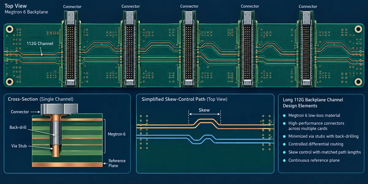
Pair skew is not only a length-matching problem. A differential pair that moves between broadside and edge-coupled regions, crosses a plane opening, or sees different glass bundles can accumulate phase error even when its CAD lengths match. Keep the pair on layers with the same reference distance, use symmetrical escape geometry, and document every allowed transition. The PCB layout review should show the pair, its reference planes, the anti-pad, and nearby return vias in one view.
For a Megtron 6 PCB backplane, lock the glass style and pressed dielectric before final equalization. If the fabricator proposes a different construction to improve availability, rerun the impedance and skew review instead of treating the substitution as a purchasing-only change.
Make via transitions and reference planes repeatable
Every backplane via is a three-dimensional discontinuity. Pad diameter, antipad shape, barrel length, back-drill depth, and the distance to the reference plane all affect local impedance. Keep breakout geometry symmetric across lanes, remove unused stubs where the channel model shows a resonance, and place return vias close enough that current does not detour around a void. The high-speed PCB manufacturing release should call out drill tolerance, plating thickness, and the back-drill datum rather than leaving them implicit.
Plane continuity is equally important. A pair that changes layers without a nearby return path can excite common-mode conversion and increase crosstalk into adjacent lanes. Use stitching vias at connector fields and maintain a continuous ground reference through the launch. The Megtron 6 materials page can confirm the material family, while the released stackup must define the actual construction and layer-to-layer transition.
Correlate the model with coupons and assembly constraints
A useful coupon is not a generic trace placed at the edge of a panel. Its layer, dielectric, copper, via, and connector-launch geometry should represent the product path that consumes the margin. Define the test method, coupon location, and acceptance window before fabrication. A cross-section plan should verify finished dielectric thickness, copper balance, plated holes, and registration around the dense connector field.
The diagram below is a conceptual verification workflow. It connects model assumptions to inspection evidence; it is not a measured customer result.
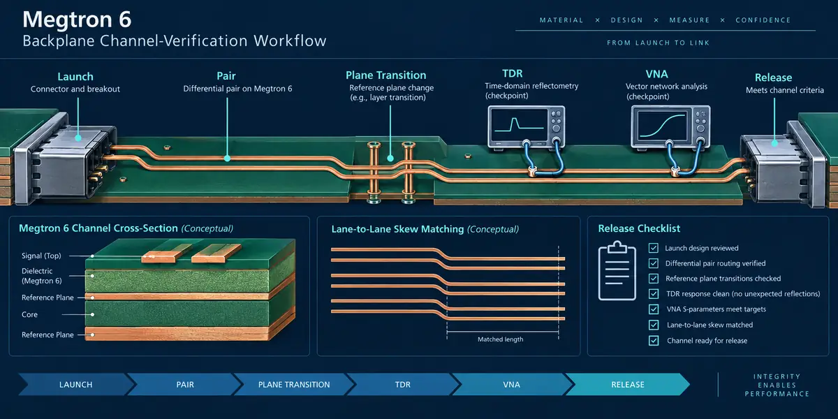
During assembly, connector coplanarity, solder-mask clearance, and reflow exposure can change the launch geometry. Coordinate the PCB assembly drawing with the RF stackup so a keep-out or paste change does not move a return path. For early builds, PCB prototype assembly can expose mechanical interference before the backplane is released to volume.
At system integration, the backplane review should also record where equalization margin is expected to absorb connector and package variation. A practical Megtron 6 PCB release separates the lane budget by segment: package breakout, board trace, via field, connector, and the mating board. This makes a late stackup or back-drill change traceable instead of forcing the team to repeat the entire analysis. If the first build exposes a launch discontinuity, revise the controlled drawing, coupon geometry, and assembly note together so the next panel is judged against one coherent revision.
Project release checklist
- One controlled stackup revision with material grade, glass style, pressed thickness, and copper range.
- Skew, impedance, insertion-loss, and crosstalk targets separated from acceptance limits.
- Via pad, antipad, back-drill, return-via, and connector-launch rules shown on the layer drawing.
- Coupon geometry and measurement method tied to the product lane and panel location.
- Assembly keep-outs, connector coplanarity, and paste or mask changes reviewed with SI.
- Material or fabrication substitutions routed through engineering change control.
For purchasing, the Megtron 6 PCB stackup, coupon drawing, and inspection plan should travel as one release package. The Megtron 6 PCB release record should carry the same construction revision. The final design review should confirm that the Megtron 6 PCB process window still supports the lane budget after panelization and drill compensation.
Panelization is another hidden variable in a backplane build. Keep high-speed lanes away from routable breakaway tabs, tooling holes, and copper thieving features that can disturb the local reference plane. When the panel drawing changes, review the lane-to-edge distance and the coupon position with the same stackup revision used for the product. This is especially important when several connector fields share a panel because drill compensation and registration can vary with local copper density.
For a controlled pilot, define the evidence package before the fabricator starts: released layer data, impedance targets, drill and back-drill notes, coupon map, cross-section request, and assembly keep-outs. The project manager can then compare the first-article package with the approved baseline without relying on informal email assumptions. A change is acceptable only when its electrical effect, manufacturing tolerance, and verification method are recorded together.
Sources: Panasonic Industrial Devices MEGTRON 6 family and R-5775/R-5670 technical data; supporting high-speed interconnect guidance from Analog Devices and Qorvo application material; KKPCB verified pages for manufacturing, layout, assembly, prototype assembly, and MEGTRON 6 material capability. Values are typical or design-reference values unless a released drawing defines the acceptance limit.
