
Table of Contents
- PTFE drilling and stackup
- RF drill table and transition geometry
- Desmear and plating controls
- Coupons and assembly handoff
A via can pass an electrical design review and still become the first reliability escape in a PTFE-based RF build. Drill wander on a Taconic RF-35 PCB, smear removal, rough hole walls, poor copper coverage, or an undersized annular ring can change both the RF transition and the mechanical life of the board. A controlled Taconic RF-35 PCB release connects the drill table, plating process, coupon, and inspection plan before the panel enters production.
Why Taconic RF-35 PCB PTFE drilling needs a different release conversation
PTFE and ceramic-loaded RF laminates do not behave like a generic FR-4 stack during drilling and desmear. The tool, feed, speed, entry material, and cleaning sequence influence hole-wall quality. A transition that looks acceptable in a 2D layout can show a larger impedance discontinuity when the barrel is not centered in the pad or when the reference-plane clearance is irregular.
Taconic RF-35 PCB documentation should identify the RF layers, dielectric thickness, finished hole, pad diameter, antipad diameter, and any back-drill or via-in-pad requirement. Public supplier data often lists RF-35 z-axis CTE around 64 ppm/°C as a typical value; it is useful for a reliability discussion, but it is not a substitute for the finished stackup and plating specification.
| Via release item | Typical project risk | Control to document |
|---|---|---|
| Finished hole | Drill wander shifts the RF centerline | Drill tolerance and inspection method |
| Annular ring | Registration loss reduces barrel capture | Minimum ring by layer and panel zone |
| Antipad | Clearance changes capacitance and phase | Layer-specific antipad geometry |
| Plating | Thin or uneven barrel copper shortens life | Plating target and coupon evidence |
Match the drill table to the RF transition
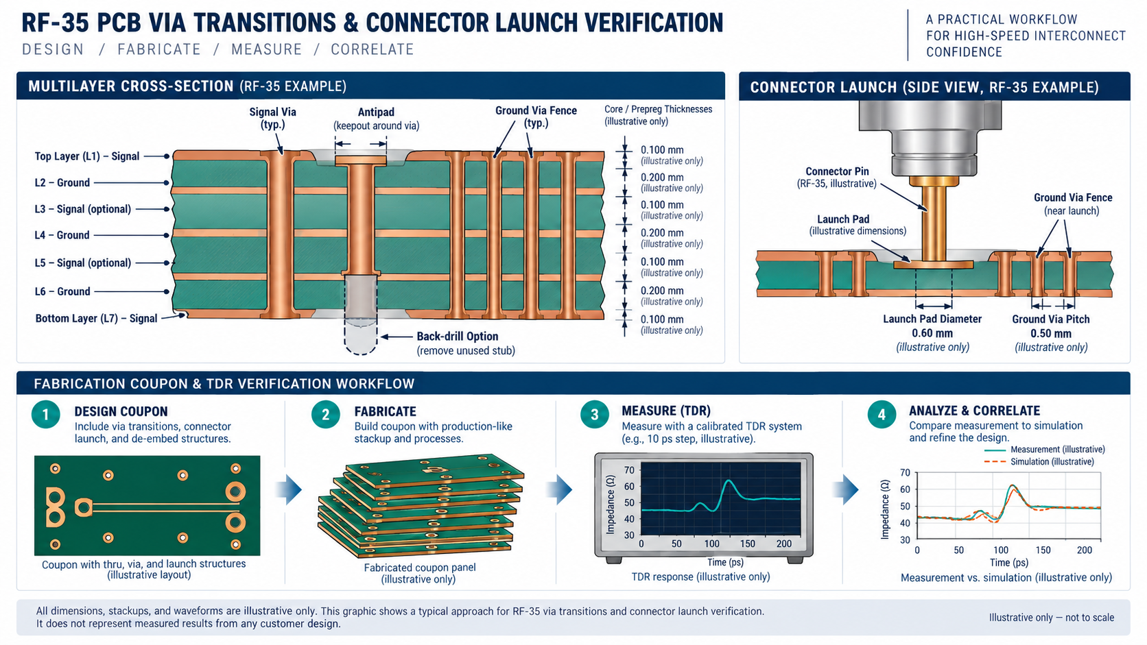
Do not release only a generic drill file for a Taconic RF-35 PCB. Mark which holes are RF transitions, which are ground stitching, and which are mechanical or assembly holes. The RF class may need a tighter finished-hole tolerance, a specific antipad, or a back-drill depth that is different from the digital portion of the board.
Use a cross-section view to show the intended barrel length and the unused stub. The transition should be reviewed in the same stackup model used for impedance. A PCB design review can also identify whether a ground via fence is close enough to contain the return current without creating an unwanted capacitive pocket.
When the RF path changes layers, add a mirrored coupon or a small connectorized test structure. It should reproduce the finished pad, antipad, via field, and adjacent ground copper. That is more informative than measuring a straight line coupon when the project risk is a launch or layer transition.
Control desmear, plating, and barrel quality
PTFE drilling often requires a process window that protects the hole wall without damaging the surrounding resin system. The supplier handoff should define the cleaning sequence, desmear intent, activation, electroless copper, and electrolytic plating targets. The exact numbers should come from the qualified process rather than being invented in the drawing.
For a Taconic RF-35 PCB, inspect representative holes at the panel location that sees the most challenging registration. A cross-section can reveal voids, nodules, cracks, or a thin corner in the barrel. If the board includes many sequential RF transitions, sample selection should include inner and outer panel positions rather than a single convenient coupon.
Use coupons that prove the real failure modes
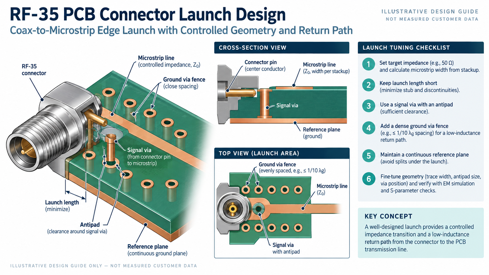
A production Taconic RF-35 PCB coupon should contain at least one representative RF via, a ground-via fence, and a connector or probe interface when those features dominate the design. Tie the coupon to the lot and panel ID. Record the drill tool, finished hole result, cross-section location, and impedance or insertion-loss result with the method used.
These records help the Taconic RF-35 PCB team separate a material issue from a registration issue. A good coupon is not a decorative extra; it is the shortest path to an evidence-based disposition when the first article is late.
Make the release usable for assembly and service
Connector and assembly drawings for a Taconic RF-35 PCB should show the keep-out around the via field, the solder-mask opening, and the inspection access. A PCB assembly supplier needs to know whether a connector is hand-installed, reflowed, or mechanically pressed after soldering. If the assembly process can load the board near a thin RF transition, include a handling note.
The final Taconic RF-35 PCB handoff should include the stackup, drill table, RF via class, plating and cross-section acceptance, coupon drawing, and a clear nonconformance path. That package prevents a via-reliability escape from being discovered only after the board is inside a fielded wireless product.
For final sign-off, add a via reliability checkpoint, a controlled-impedance PCB transition note, and an RF PCB manufacturing inspection record.
Sources: public RF-35 supplier data for typical thermal and electrical properties; Analog Devices RF transition and return-path guidance; KKPCB drilling, plating, and inspection workflow information reviewed for this article.
