
Beamforming boards are often released as if they were ordinary controlled-impedance backplanes. That shortcut is risky. In a multi-channel array, a small phase error in one feed path changes the composite beam, reduces calibration margin, and can look like a front-end or firmware fault. A practical Taconic RF-35 PCB workflow therefore treats phase balance as a board-level production requirement, not only a simulation result.
Why channel-to-channel phase balance becomes a manufacturing problem
Every channel on a Taconic RF-35 PCB contains more than a copper length. The electrical path includes the RF trace, reference-plane transition, plated vias, connector launch, solder mask boundary, and the local laminate stack. A beamforming designer may equalize CAD lengths while two channels still differ because the finished copper width, dielectric height, or via barrel geometry is not identical. The risk grows when the array combines edge launches with internal layer transitions.
Start the release with a channel budget: allowable phase skew, amplitude variation, routing-length tolerance, connector repeatability, and calibration range. Record which terms are design targets and which are to be confirmed on a production coupon. This prevents a project team from treating a nominal field-solver output as a guaranteed board measurement.
Build an electrical-length budget before routing the array
Use the supplier’s typical RF-35 electrical data as a starting point, then freeze the actual construction with the fabricator. Public RF-35 data commonly lists a typical Dk near 3.50 and Df near 0.0018 at a stated test frequency; those are material reference values, not a promise that every finished trace has the same effective permittivity. Finished copper profile, glass style, resin distribution, trace etch, and solder-mask treatment still influence phase.
| Release item | What the engineer should control | Evidence to request |
|---|---|---|
| RF trace | Width, spacing, corner treatment, and finished copper target | Stackup drawing and impedance model |
| Reference plane | Continuous ground under every array feed | Layer review with return-path markup |
| Transition | Via antipad, back-drill rule, and launch geometry | Drill table plus transition coupon |
| Array symmetry | Matched geometry and repeatable fan-out | Channel-to-channel CAD comparison |
Choose a Taconic RF-35 PCB stackup that protects the return path
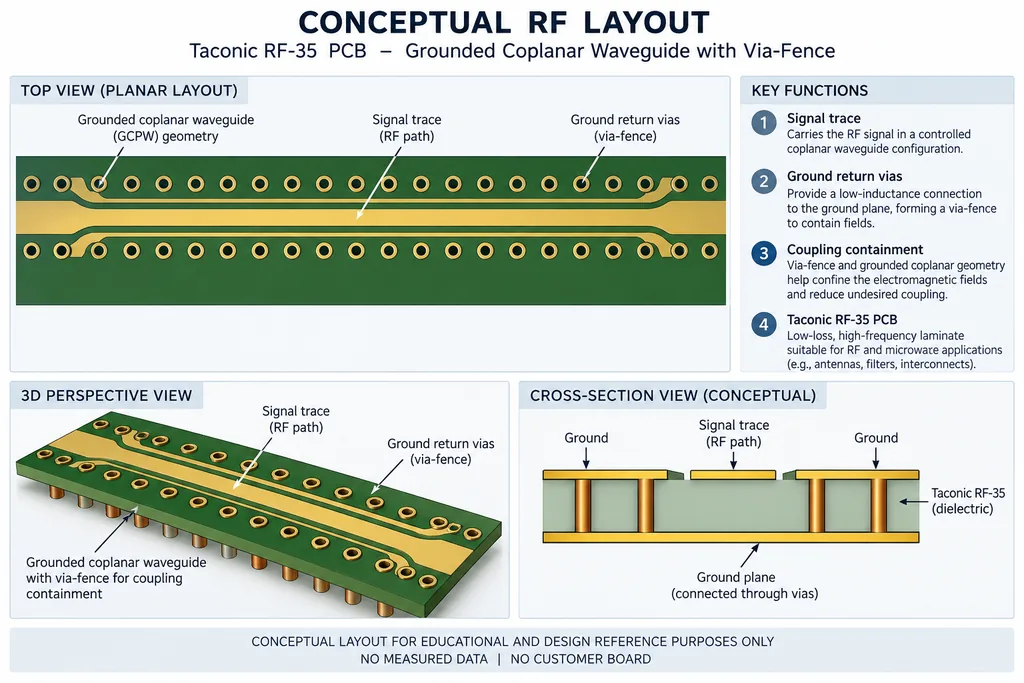
For each Taconic RF-35 PCB channel, keep the signal-to-reference spacing stable and avoid plane voids beneath the feed. A coplanar waveguide may be attractive for connector access, while a stripline section can improve shielding through the array. The handoff must show where the geometry changes and how the return current crosses the transition.
Use ground vias as a repeatable fence rather than as decoration. Their pitch, distance from the RF edge, and connection to the intended reference plane should be dimensioned. If a channel crosses a split, a mounting hole, or a dense digital escape region, the phase budget should be recalculated. Analog Devices RF layout guidance emphasizes continuous reference planes and short, low-inductance return paths for exactly this reason.
On a multilayer build, coordinate RF layers with power and digital layers early. KKPCB’s PCB design review can flag a return-path interruption before the array is routed. The goal is not the thinnest stackup; it is a construction that the fabricator can hold consistently over the panel.
Route array feeds for assembly and calibration repeatability
Connector launches should be copied from a controlled reference geometry. Keep the launch, anti-pad, and first bend in the same coordinate relationship for every channel. Avoid placing a solder-mask edge or silkscreen feature inside the launch field. For populated modules, leave a mechanical keep-out around the connector and allow the assembly team to inspect the ground-via fence after reflow.
A phased-array program built on a Taconic RF-35 PCB also needs a calibration strategy. Put calibration couplers or test pads where they can be probed without disturbing the active feed. If the board is calibrated after assembly, document the connector torque method, cable reference plane, and fixture de-embedding. This is where a Taconic RF-35 PCB must be treated as a calibrated channel set rather than a collection of independent traces. These controls turn a phase-balance goal into a repeatable production decision.
Release the array with evidence the project team can use
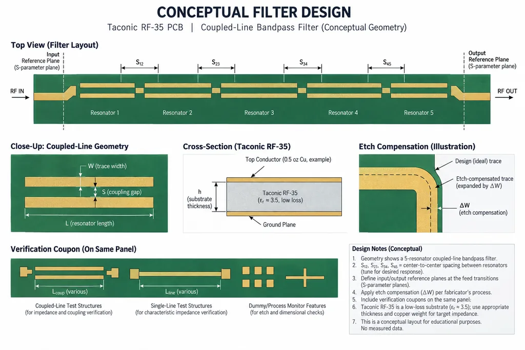
A supplier-ready PCB manufacturing package for a Taconic RF-35 PCB should contain the controlled stackup, RF net classes, finished-copper assumptions, via and back-drill rules, coupon intent, and acceptance limits. Mark any values that are targets rather than measurements. A production Taconic RF-35 PCB coupon should mirror the most sensitive trace width, dielectric height, and transition used in the beamforming path; a generic coupon can hide the actual risk.
For a build that combines RF layers, digital control, and dense power distribution, a structured PCB fabrication capability review is more useful than a late material substitution. Ask for panelization notes, registration strategy, inspection access, and a clear response when a measured result falls outside the phase or impedance window.
The best Taconic RF-35 PCB release is one that lets design, sourcing, and test teams make the same decision from the same evidence. When those controls are in place, a Taconic RF-35 PCB can support a multi-channel beamforming network without relying on hidden tuning or unexplained channel offsets.
For downstream handoff, pair the release with RF PCB design notes and an PCB assembly inspection view so the same phase-critical geometry is preserved after fabrication.
Sources: public RF-35 supplier data for typical electrical properties; Analog Devices RF PCB layout guidance and RF/mixed-signal application notes; KKPCB process and capability information reviewed for this engineering workflow.
