
Ku-band TLY-5 PCB projects need a finished-board reference, not only a laminate name.
Table of Contents
TLY-5 PCB is often selected for a Ku-band front end because the laminate combines a low nominal dielectric constant with low dielectric loss. The difficult part is not choosing a low-loss material on a schematic. It is preserving the launch geometry, copper surface condition, and phase repeatability after lamination, etching, plating, and connector assembly.
For an RF engineer, the project risk appears as excess insertion loss or a phase shift between nominally identical channels. For a project manager, the same risk appears later as a tuning loop, an ECO, or a second prototype build. This article explains how to release a Ku-band front-end board around the material properties that actually move the result.
Table of Contents: Finished-board sensitivity; copper roughness; connector launch; phase repeatability; manufacturing handoff; release checklist.
Why Ku-band performance is sensitive to the finished board
At Ku-band, the electrical length of a short launch is large enough that small geometry changes can become a measurable phase error. The finished dielectric thickness, copper profile, trace width, reference-plane spacing, via barrel, solder mask condition, and connector datum all participate in the transition. A nominal material callout is therefore only the starting point for high-frequency PCB design.
TLY-5 is commonly described with a nominal Dk near 2.20 and a low Df near 0.0009 in published typical data. Those values are useful for first-pass modeling, but the released stackup should use finished dielectric targets and the construction that the fabricator can hold. Do not silently mix a supplier’s nominal Dk with a press thickness that was never verified.
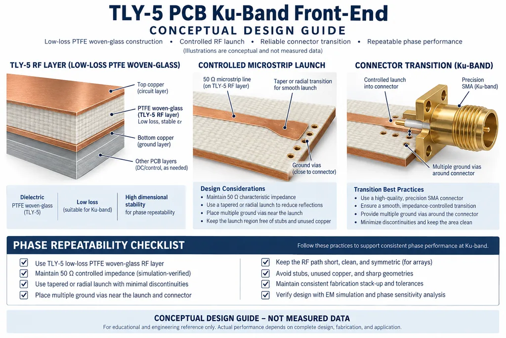
Control copper roughness before it becomes a loss surprise
Copper roughness changes the effective path seen by a high-frequency current. A smoother foil can reduce conductor loss, but the improvement should be considered together with copper thickness, etch compensation, peel strength, and the selected surface finish. The correct procurement question is not “which copper is smoothest?” It is “which finished copper and process window can be repeated on the released geometry?”
Build a copper assumption into the field-solver model and keep it visible in the stackup record. If the design uses a narrow microstrip or grounded coplanar line, define the finished trace width after etch and plating rather than only the artwork width. This gives the controlled-impedance PCB review a real acceptance point.
Release the connector launch as a mechanical and RF feature
A Ku-band launch should be dimensioned from a connector datum, not from an arbitrary board edge. The launch drawing should specify pad length, antipad diameter, reference-via spacing, solder-mask opening, and the keep-out around the connector body. If the connector is installed during assembly, coplanarity and solder fillet shape also belong in the review.
Use a short back-drilled or blind transition only when the layer sequence and fabrication capability justify it. A via that is electrically acceptable in simulation can still fail production correlation if its registration, plating thickness, or stub length moves outside the modeled window. The PCB manufacturing traveler should therefore carry the launch drawing, drill table, and inspection datum together.
In a production TLY-5 PCB release, the TLY-5 PCB trace model, TLY-5 PCB connector datum, and TLY-5 PCB coupon must stay aligned. The TLY-5 PCB inspection record should show which values are typical and which are controlled targets.
Ku-band TLY-5 PCB Phase Repeatability
Use phase repeatability as the acceptance metric
For a multichannel front end, insertion loss alone is not enough. The release plan should define a phase target, the reference plane, the test fixture, and the calibration method. A practical engineering estimate is to calculate the phase sensitivity to finished dielectric thickness and trace length, then allocate a portion of the total budget to fabrication and another portion to assembly.
For example, if a short transition is estimated at 25 mm electrical length and the design team allocates a 3-degree phase window, the stackup review should show how much of that window is consumed by dielectric thickness, copper geometry, connector placement, and test repeatability. That is a design target, not a KKPCB measured result. The useful output is a traceable allocation that tells the team what to inspect when the phase result moves.
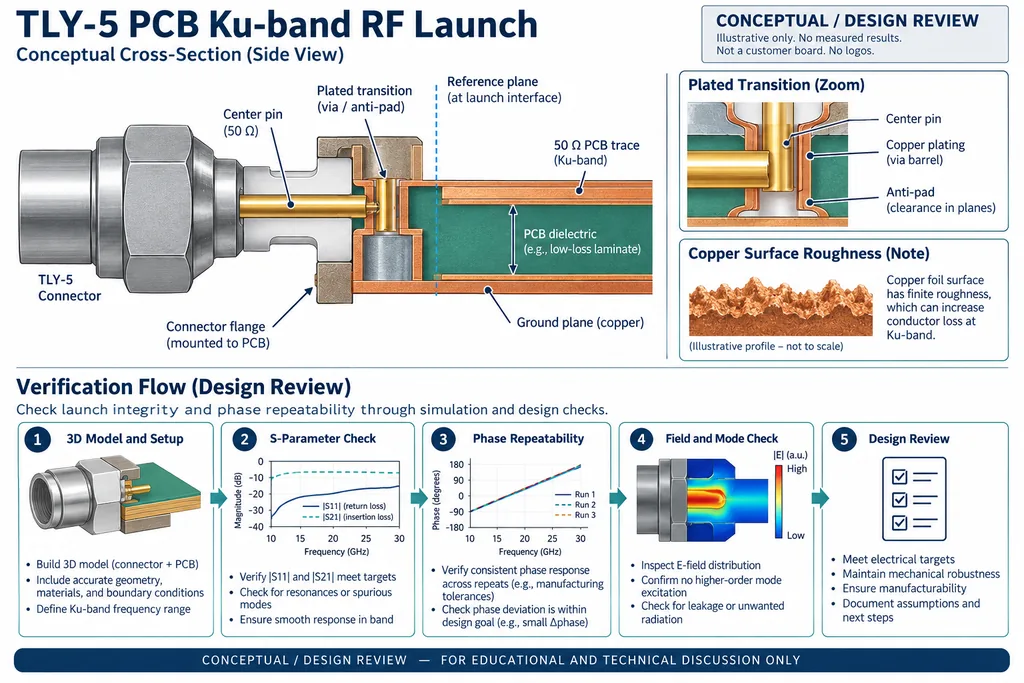
The TLY-5 PCB laminate should be treated as part of the launch system, not as a catalog substitution. A TLY-5 PCB stackup review ties the TLY-5 PCB dielectric target to the actual copper and connector geometry. When a TLY-5 PCB build is released with those assumptions visible, the RF team can isolate material variation from assembly variation. That is why TLY-5 PCB documentation belongs in the same revision package as the launch drawing.
Manufacturing and assembly handoff
For a repeatable build, provide the RF PCB materials callout, finished dielectric targets, copper assumptions, drill tolerances, and surface-finish requirements in one controlled package. Add a coupon or witness structure that represents the critical line and launch. The coupon should be traceable to the same panel, material lot, and press cycle as the product feature.
During assembly, protect the RF launch from unnecessary rework. Define connector placement tolerances, inspection points, cleaning limits, and a rework disposition rule. A board that passes bare-board inspection can still lose phase consistency if the connector is shifted or the solder fillet changes the reference plane. The PCB assembly handoff should include the RF drawing rather than treating the connector as an ordinary mechanical part.
For project release, the TLY-5 PCB drawing, TLY-5 PCB stackup, and TLY-5 PCB inspection plan should share one revision. This keeps the TLY-5 PCB decision traceable when a Ku-band prototype moves into production.
A practical release checklist
- Finished dielectric targets are recorded for the RF layer pair.
- Copper roughness and thickness assumptions match the released model.
- Connector datum, via transition, antipad, and mask opening are dimensioned.
- Coupon geometry represents the critical Ku-band path.
- Phase, insertion loss, calibration plane, and fixture are defined before testing.
- Material lot, panel location, drill revision, and assembly revision are traceable.
For procurement and release, keep the TLY-5 PCB material callout tied to the finished stackup. The TLY-5 PCB impedance review should use the same copper and dielectric assumptions, while the TLY-5 PCB launch drawing keeps the RF and mechanical datums aligned.
Sources: Taconic TLY-5 typical material data; IPC-TM-650 methods relevant to dielectric, copper, drilling, plating, registration, and impedance verification; RF component application guidance from Qorvo and Analog Devices; KKPCB high-frequency PCB engineering and manufacturing capability notes. Values in this article are typical, target, or calculated references unless explicitly identified as measured.
