
Mixed RF-and-digital boards rarely fail because the engineer forgot a trace-width rule. They fail when the stackup, plane strategy, and return path are treated as separate documents. This article uses an RF-35 PCB example to explain how a project team can partition RF and digital functions while keeping the board manufacturable.
RF-35 ceramic-filled PTFE/glass materials are selected for their microwave behavior, but the laminate does not remove the need for disciplined reference planes. Supplier typical data such as Dk near 3.50 at 1.9 GHz is a starting point. The released design still depends on the approved stackup, pressed dielectric thickness, copper state, and via geometry.
1. Partition the RF-35 PCB stackup
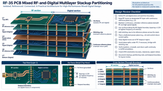
Begin with layer ownership rather than component placement. Assign one or more RF routing layers, an adjacent continuous reference plane, digital routing layers, and a power strategy that does not force high-speed return current through the RF region. On an RF-35 PCB, a thin controlled dielectric between an RF signal and its plane can be valuable, but only if the fabricator can hold the finished spacing across the panel.
- Place RF signal layers next to continuous ground references.
- Keep high-speed digital layers away from connector launches and antenna feeds.
- Reserve plane layers for a defined purpose instead of using arbitrary copper fills.
- Document where stitching vias connect the RF and digital reference systems.
A mixed-signal PCB design review should show the field path and the DC return path together. A split plane under a high-speed transition can force current around the split and create common-impedance coupling even when the nominal trace impedance is correct.
2. Protect RF-35 PCB return paths
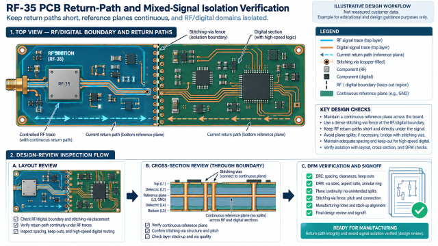
For an RF-35 PCB, the return path is part of the transmission line. Keep reference copper continuous below RF traces, provide stitching vias where a transition changes layers, and avoid unnecessary antipad enlargement. If a digital route must cross a boundary, identify the reference plane it uses and provide a controlled bridge rather than allowing the current to search for a distant path.
Return-path review questions
| Review item | Failure mode | Design response |
|---|---|---|
| Plane continuity | Return current detours around a split or void. | Move the split, reroute the signal, or add a controlled stitching strategy. |
| Via fence | RF energy leaks into the digital region. | Define fence pitch and ground-layer connections with DFM clearance. |
| Power transition | Noise couples into the RF reference. | Use local decoupling and keep power vias outside the launch field. |
| Shield boundary | Shield wall interrupts the intended return path. | Connect the shield to the correct planes and document openings. |
Link the electrical intent to the approved RF PCB materials. Glass style, resin content, and pressed spacing affect the field distribution, so the same line geometry should not be assumed for every RF-35 PCB construction.
3. Define the RF/digital boundary
The boundary is more useful when it is drawn as a design rule instead of a visual line. Mark the keepout for digital traces, clocks, switching nodes, and noisy power components. Then define where the RF-35 PCB ground fence and stitching vias are allowed to sit. A boundary that is too close to a connector may violate annular-ring or assembly clearances; one that is too far away may fail to contain the field.
Use the boundary to coordinate placement, routing, and enclosure features. A mounting hole, shield tab, or heatsink can remove copper exactly where the RF return path needs it. Call out those exceptions in the drawing and include them in the DFM review.
4. Verify the design before release
Simulation can compare alternative fence pitches, launch clearances, and layer transitions, but a model is not a production measurement. Use simulation to choose a robust geometry, then place a representative coupon that exposes the critical RF layer pair and return-path features. The coupon can support cross-section review and an agreed impedance method without being presented as a customer result.
Review the RF-35 PCB with layout DRC, plane-isolation checks, cross-section targets, and a fabrication drawing that names the reference planes. A PCB manufacturing traveler should carry the same revision as the stackup and impedance table. KKPCB can review a mixed-signal stack and flag drill, registration, or press-sequence risks before tooling.
5. Complete the manufacturing handoff
The assembly team also needs the boundary rules. Share paste restrictions around RF launches, shield installation order, no-rework zones, and inspection access with the PCB assembly team. Rework heat, excess solder, or a misplaced shield spring can alter the RF return path after fabrication is complete.
For complex builds, KKPCB states capability up to 62 layers and 8 sequential lamination steps. That supports separated RF, digital, and power structures, but each program still needs a realistic layer map, panel plan, and registration budget. In summary, a reliable RF-35 PCB is a system of controlled interfaces: stackup, plane continuity, boundary, via fence, coupon, and assembly notes.
Sources: Taconic RF-35 and RF-35P processing guidance and typical property tables; IPC-TM-650 references for impedance and cross-section evaluation; and KKPCB manufacturing capability notes. Typical values are reference data rather than customer measurements; confirm the current supplier datasheet and lot before release.
