
Reliable RF transitions are often lost at the connector, launch, or layer change rather than in the long transmission line. This guide shows how an RO4350B PCB project can use via fences, reference-plane continuity, and fabrication controls to protect return current. It is an engineering design method, not a claimed KKPCB customer result.
Why the transition is the risk point
A coax launch, edge connector, or vertical via changes field distribution in a short distance. The RO4350B PCB trace may meet a calculated width, yet the transition can add inductance, excess capacitance, and a return-current detour. Define the launch as a complete structure: signal pad, antipad, nearby ground vias, reference planes, solder mask, and connector keep-out.
| Transition item | Common failure | Design action |
|---|---|---|
| Signal via | Long unused barrel resonates above the operating band. | Back-drill or set a controlled via depth when the released process allows it. |
| Ground-via fence | Return current spreads before reaching the next plane. | Place a regular fence beside the launch and verify drill clearances. |
| Reference plane | Anti-pad or split interrupts the return path. | Show plane voids and the continuous return layer on the stackup review. |
| Solder mask | Mask dam changes local capacitance at the pad. | Call out mask expansion and keep the RF launch geometry controlled. |
Build the return-current path first
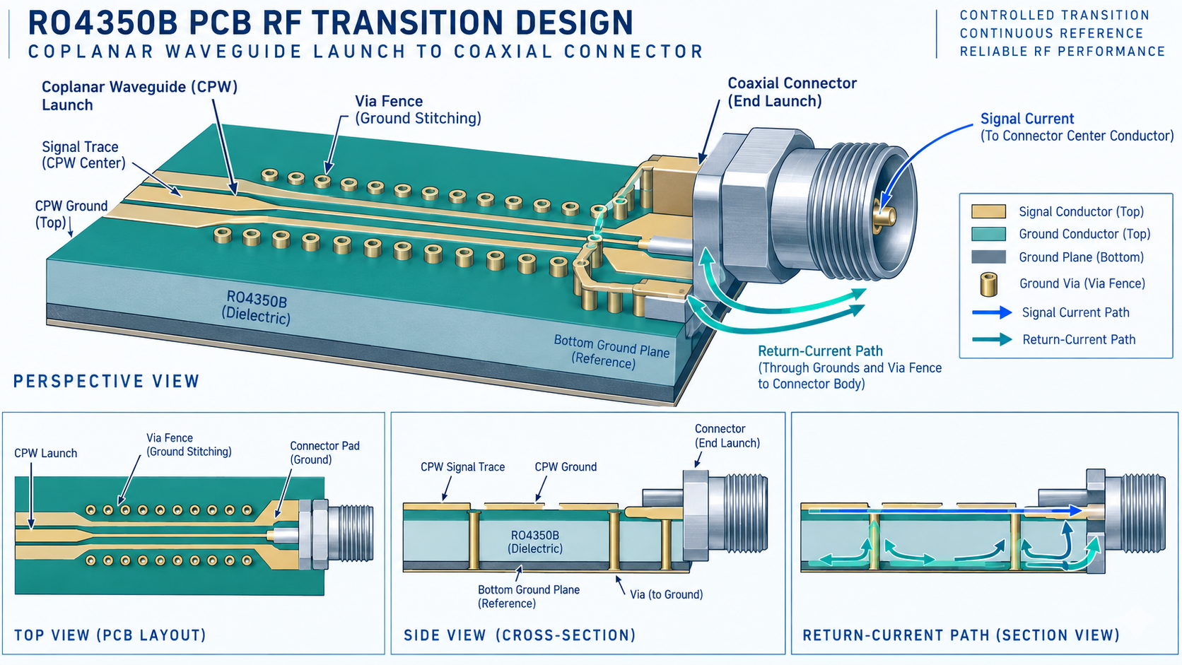
On an RO4350B PCB, mark the closest solid reference plane for every RF segment. Ground vias should connect that plane without forcing current around a void or mounting hole. A controlled impedance PCB rule is incomplete if the reference-plane transition is undefined.
Via-fence spacing decisions
Fence pitch should be selected against the highest relevant frequency, trace-to-fence spacing, drill tolerance, and keep-out around the connector. Avoid presenting a single universal millimeter value; the correct pitch depends on the stackup and process. The RO4350B PCB drawing should define the intent, and the fabricator should confirm annular ring, registration, and hole-to-copper capability.
Control the launch geometry
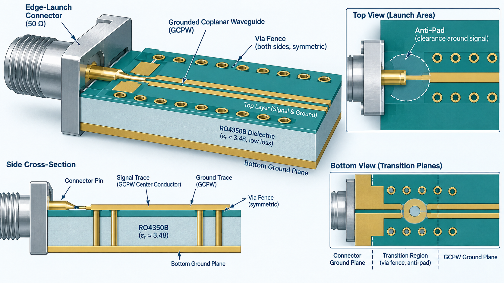
Keep the signal via short, reference its antipad to the actual plane pair, and avoid abrupt neck-downs. For edge launches, align the connector ground tabs with the board ground-via fence. For SMP or similar coax launches, include the connector footprint as part of the electromagnetic model. If a multilayer PCB changes plane order, re-check the launch rather than copying the old footprint.
Manufacturing checks that protect RF behavior
During PCB manufacturing review, compare drill data, copper layers, plane voids, solder-mask openings, and connector dimensions. Registration error can move a via fence relative to the trace; etch variation can alter a narrow launch neck. Release the finished dielectric target, copper profile, surface finish, and drill tolerance instead of relying on a generic RO4350B PCB note.
Illustrative project failure investigation
Consider a radar front-end prototype whose long traces pass simulation but whose measured return loss degrades after a connector change. This is an illustrative scenario, not a KKPCB case. The team should inspect the launch footprint revision, ground-via fence, anti-pad, unused barrel, and reference-plane continuity before changing the laminate. A project manager should require a transition drawing and controlled ECO for every connector or layer-change revision.
Verification sequence
- Identify every RF launch, via transition, and plane change.
- Document signal-via depth, antipad, ground-via fence, and keep-outs.
- Re-solve the transition with finished dielectric and copper assumptions.
- Review drill, registration, etch, and solder-mask tolerances with the fabricator.
- Use an approved coupon or fixture only when the quality record contains the result.
Release checklist
- The RO4350B PCB drawing names the exact transition stackup and plane pair.
- Each RF launch has a defined signal-via and ground-via pattern.
- The HDI PCB escape keeps microvia fields away from critical launch antipads.
- Any PCB materials substitution triggers a new transition review.
- The PCB manufacturing drawing identifies finished tolerances and acceptance ownership.
Questions engineers ask
Does a wider trace fix a poor launch?
No. Launch behavior is set by the complete signal and return structure, not width alone.
Should every fence use the same pitch?
No. Use the electrical wavelength, geometry, and manufacturability to choose a documented pitch.
When is back-drilling justified?
When the unused via barrel is electrically significant and the released RO4350B PCB process can control the depth and inspection.
Sources: Rogers RO4350B manufacturer data provide vendor-typical material context; KKPCB public High-Frequency PCB, PCB Materials, HDI PCB, Multilayer PCB, and PCB Manufacturing pages verify service categories. This article contains no external hyperlinks and no claimed customer measurement.
Transition sign-off for the RO4350B PCB
Use a named review owner for every connector and layer change. The RO4350B PCB release should show the signal reference plane, the ground-via fence, the antipad, and the approved drill class. If a component vendor changes the launch footprint, update the RO4350B PCB field model and the assembly drawing together. Keep the RO4350B PCB acceptance note tied to a revision-controlled coupon or fixture so that production questions can be answered without guessing.
For a dense radio card, separate the RF launch review from general routing review. Check the connector datum, board edge, copper-to-edge spacing, solder-mask opening, and chassis contact. These details are practical manufacturing controls, not a substitute for measured qualification. An engineer can then hand a complete transition package to procurement and the PCB manufacturing team.
Production review note
The RO4350B PCB transition owner should confirm the connector datum, board-edge clearance, and finished dielectric before panel release. Record the RO4350B PCB via-fence pattern in the fabrication drawing and keep the RO4350B PCB revision synchronized with the test fixture.
Final RF handoff
Release the RO4350B PCB transition drawing with the stackup, and cross-check the RO4350B PCB manufacturing notes before panel release. This final RO4350B PCB review keeps the return path, launch datum, and inspection owner aligned. Record the RO4350B PCB acceptance criteria beside the connector revision so procurement and fabrication use the same controlled package.
