The Importance of RF Transceiver PCB in Wireless Electronics
Modern wireless communication systems rely heavily on high-performance RF transceiver circuits to enable:
- Signal transmission
- Signal reception
- Data communication
- Wireless connectivity
As technologies continue advancing toward:
- 5G and 6G communication
- IoT devices
- Automotive radar systems
- Satellite communication
- Smart wireless modules
the complexity of RF Transceiver PCB design continues to increase.
Unlike standard PCB designs, RF transceiver PCBs must handle:
- High-frequency RF signals
- Ultra-low signal loss
- Sensitive analog and digital integration
- Strict EMI and signal integrity requirements
At KKPCB, RF PCB solutions are optimized for:
- Stable wireless communication
- High-frequency signal integrity
- Low-noise RF performance
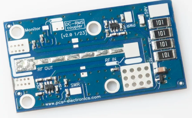
2. What Is an RF Transceiver PCB?
An RF Transceiver PCB is a printed circuit board designed to support both:
- RF signal transmission
- RF signal reception
within wireless communication systems.
Typical RF transceiver PCB modules include:
- RF power amplifiers (PA)
- Low-noise amplifiers (LNA)
- RF filters
- Mixers
- Oscillators
- Antenna matching circuits
- RF transceiver ICs
These PCB systems are widely used in:
- Wireless communication modules
- Wi-Fi and Bluetooth devices
- Cellular communication systems
- RF sensing equipment
3. Key Challenges in RF Transceiver PCB Design
3.1 High-Frequency Signal Integrity
RF signals are highly sensitive to:
- Impedance discontinuities
- Transmission loss
- Reflection and crosstalk
Maintaining stable RF signal transmission is critical for:
- Communication range
- Data accuracy
- RF efficiency
3.2 EMI and Noise Interference
RF transceiver circuits often combine:
- Analog RF signals
- High-speed digital signals
- Power circuits
This increases the risk of:
- Electromagnetic interference (EMI)
- Noise coupling
- Signal distortion
Proper PCB layout and grounding are essential.
3.3 Thermal Management
RF power amplifiers and transceiver ICs generate concentrated heat.
Without proper thermal management:
- RF efficiency decreases
- Frequency stability is affected
- Component lifespan shortens
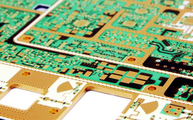
4. RF PCB Materials for Transceiver Applications
Material selection directly impacts RF performance.
Common RF PCB materials include:
- Rogers RO4350B
- Rogers RO4003C
- PTFE-based laminates
- Low-loss hydrocarbon ceramic materials
Key material requirements:
- Low dielectric loss
- Stable dielectric constant
- High thermal reliability
- Low moisture absorption
These properties improve:
- Signal transmission quality
- RF stability
- High-frequency performance
5. Controlled Impedance in RF Transceiver PCB
Controlled impedance is fundamental to RF PCB design.
Stable impedance routing helps:
- Minimize signal reflection
- Improve RF matching
- Enhance transmission efficiency
Characteristic impedance is related to transmission line structure:
Z0=LCZ_0 = \sqrt{\frac{L}{C}}Z0=CL
Common RF transmission structures include:
- Microstrip lines
- Stripline routing
- Coplanar waveguides
At KKPCB, advanced stack-up and routing optimization ensure stable RF performance.
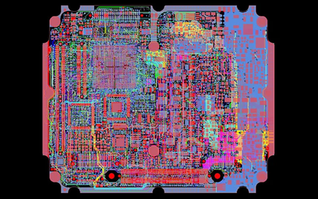
6. RF Layout Optimization Techniques
Proper RF layout is critical for minimizing loss and interference.
Best practices include:
- Short RF trace routing
- Smooth transmission path transitions
- Isolation between RF and digital circuits
- Continuous ground reference planes
- Via stitching for shielding
These techniques improve:
- RF signal integrity
- EMI suppression
- Wireless communication stability
7. EMI Shielding and Grounding Design
EMI control is one of the most important aspects of RF transceiver PCB design.
Effective strategies include:
- RF shielding cans
- Ground via fences
- Isolated RF sections
- Proper return path design
Good grounding improves:
- Noise suppression
- RF sensitivity
- Signal quality
8. Thermal Management in RF Transceiver PCB
RF power devices generate localized heat that must be efficiently dissipated.
Thermal solutions include:
- Thermal vias under RF ICs
- Copper heat-spreading planes
- Metal-backed PCB structures
- Heat sink integration
Thermal optimization improves:
- Frequency stability
- RF efficiency
- Long-term reliability
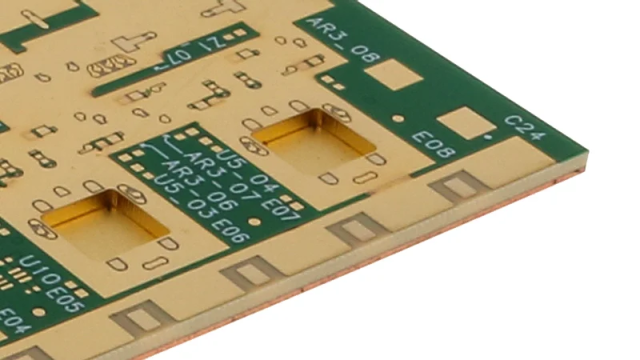
9. Manufacturing Challenges of RF Transceiver PCB
RF PCB manufacturing requires:
- Tight impedance tolerance control
- Precision etching processes
- Stable dielectric thickness
- Low-profile copper foil processing
High-frequency RF PCB fabrication must minimize:
- Signal discontinuities
- Surface roughness effects
- Manufacturing variations
At KKPCB, advanced manufacturing processes ensure:
- Stable RF performance
- High-frequency consistency
- Reliable production quality
10. Applications of RF Transceiver PCB
RF Transceiver PCBs are widely used in:
- 5G wireless communication systems
- Wi-Fi 6/7 modules
- Bluetooth and IoT devices
- Automotive radar systems
- Satellite communication modules
- Industrial wireless systems
These systems require:
- Low signal loss
- High-frequency stability
- Reliable wireless connectivity
11. Future Trends in RF Transceiver PCB Technology
Future RF PCB development focuses on:
- mmWave communication systems
- Integrated RF front-end modules
- Smaller and more compact wireless devices
- AI-driven wireless communication systems
- Advanced low-loss PCB materials
Emerging technologies require:
- Higher RF integration density
- Improved thermal efficiency
- Ultra-low signal loss performance
12. Conclusion
RF Transceiver PCB technology is essential for modern wireless communication systems requiring:
- High-frequency signal transmission
- Stable RF performance
- Low EMI interference
- High thermal reliability
Through advanced RF layout optimization, impedance-controlled design, and precision manufacturing, engineers can achieve:
- Better wireless communication performance
- Higher RF efficiency
- Long-term operational stability
With extensive expertise in RF electronics manufacturing, KKPCB provides advanced PCB solutions for next-generation wireless and RF communication systems.
