What Is a Taconic PCB?
A Taconic PCB is a high-performance RF PCB manufactured using Taconic materials, which are engineered for low loss, stable dielectric properties, and reliable high-frequency performance.
Taconic PCB materials are widely used in RF, microwave, and high-speed digital applications, where signal integrity is critical.
Common Taconic material families used in Taconic PCB design include:
- RF-35 (glass-reinforced hydrocarbon ceramic)
- TLY series (PTFE-based materials)
- TLC series (cost-optimized RF materials)
A Taconic PCB provides a strong balance between RF performance, manufacturability, and cost efficiency.
Why Taconic PCB Materials Matter
The performance of a Taconic PCB comes from its optimized material properties:
- Low Dissipation Factor (Df)
Reduces signal loss in RF PCB designs - Stable Dielectric Constant (Dk)
Ensures consistent impedance in RF traces - Wide Frequency Stability
Suitable for GHz-level applications - Good Thermal Reliability
Supports stable operation under varying conditions - Manufacturing Compatibility
Easier processing compared to pure PTFE PCB materials
These features make Taconic PCB a reliable choice for high-frequency RF PCB applications.
Taconic PCB vs Rogers PCB vs PTFE PCB
Engineers often compare Taconic PCB with other RF PCB materials:
| Property | Taconic PCB | Rogers PCB | PTFE PCB |
|---|---|---|---|
| Loss (Df) | Low | Low | Ultra Low |
| Dk Stability | High | Very High | Excellent |
| Processing Difficulty | Moderate | Moderate | High |
| Cost | Medium | High | Highest |
| Application | RF, microwave | High-end RF | Ultra-high frequency |
Key Insight:Taconic PCB offers a balance between performance and cost, while PTFE PCB targets maximum performance.
RF Design Considerations for Taconic PCB
To fully utilize Taconic PCB materials, proper RF PCB design is essential:
1. Controlled Impedance RF Trace Design
- Maintain consistent impedance across Taconic PCB layers
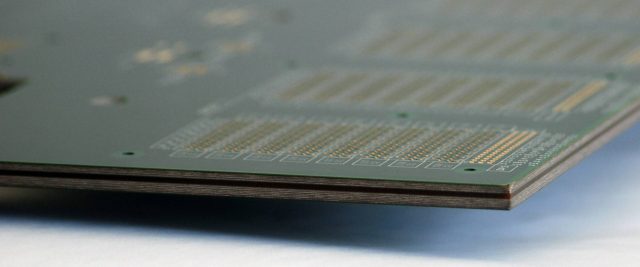
2. Stack-Up Optimization
- Use hybrid stack-ups combining Taconic material and FR-4
3. Minimize RF Trace Loss
- Keep RF traces short and direct
- Reduce via transitions
4. Grounding and Shielding
- Continuous ground planes improve RF stability
5. Surface Roughness Control
- Smooth copper improves RF signal transmission
A Taconic PCB must be designed as a complete RF system—not just a material upgrade.
When Should You Use a Taconic PCB?
Use a Taconic PCB when:
- Designing RF and microwave circuits
- Working in GHz frequency ranges
- Requiring low-loss signal transmission
- Balancing performance and cost
- Developing wireless communication systems (5G, IoT)
Avoid Taconic PCB when:
- Ultra-low loss (mmWave) is required → consider PTFE PCB
- Cost is extremely constrained → consider FR-4
- https://www.kkpcba.com/pcb-layout/Design is low-frequency
Engineering principle:
Taconic PCB is ideal when you need RF performance without the extreme cost of PTFE.
Cost Optimization Strategies
Taconic PCB offers flexibility for cost optimization:
- Use Taconic material only in RF-critical layers
- Combine with FR-4 in hybrid stack-ups
- Avoid overdesign with unnecessary RF layers
This approach helps maintain RF performance while controlling overall PCB cost.
Common Mistakes in Taconic PCB Design
Avoid these typical issues:
- Treating Taconic PCB like standard FR-4
- Ignoring impedance control in RF traces
- Overusing high-end materials unnecessarily
- Poor stack-up planning
- Not considering manufacturing tolerances
These mistakes can reduce the performance advantage of Taconic PCB.
Final Thoughts
Taconic PCBs are a powerful solution for RF and high-frequency PCB design, offering a strong balance between performance, manufacturability, and cost.
Their success depends on:
- Proper material selection
- Optimized RF trace design
- Balanced stack-up strategy
- Manufacturing-aware design
At KKPCB, we provide Taconic PCB manufacturing and RF design support, helping customers achieve reliable high-frequency performance with optimized cost efficiency.
