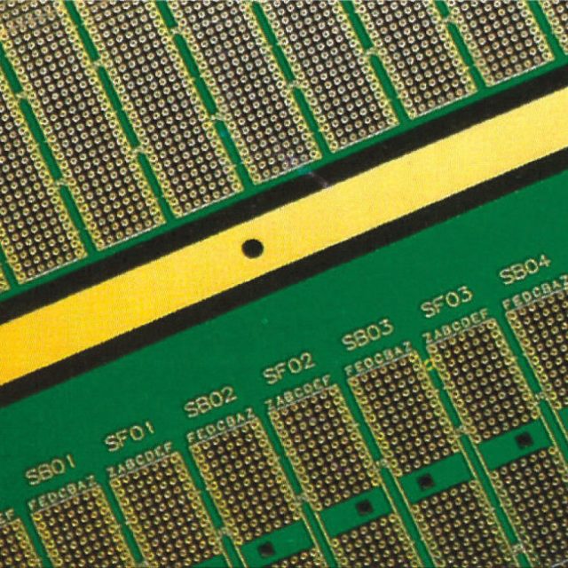
What Is a Fine Line PCB?
A Fine Line PCB refers to a board manufactured with extremely narrow trace width and spacing, typically:
- ≤100 µm (4 mil) → standard fine line
- ≤75 µm (3 mil) → advanced
- ≤50 µm (2 mil) or below → ultra-fine line
These geometries go beyond conventional PCB fabrication limits and require advanced imaging, etching, and process control.
Fine line technology is a key enabler for HDI designs, high pin count devices, and compact electronic systems.
Why Fine Line PCBs Are Needed
As component density increases, especially with fine-pitch BGAs and compact modules, routing space becomes extremely limited.
Fine line PCBs help solve this by:
- Increasing routing channels between pads
- Reducing the need for additional layers
- Supporting high pin count device breakout
- Enabling compact and lightweight designs
In many modern designs, especially in mobile, AI hardware, and high-speed systems, fine line capability determines whether a layout is feasible or not.
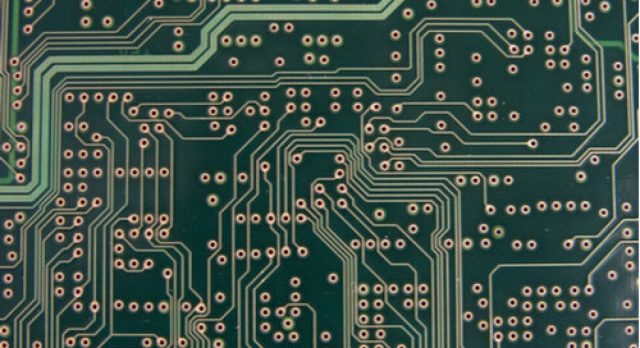
Manufacturing Limits: Where Reality Begins
Fine line design is heavily constrained by manufacturing capability.
Key process challenges include:
- Etching Accuracy:
Narrow traces are sensitive to over-etching and undercutting - Imaging Resolution:
Requires advanced LDI (Laser Direct Imaging) systems - Copper Thickness Control:
Thicker copper makes fine lines harder to achieve - Registration Accuracy:
Layer-to-layer alignment must be extremely precise - Yield Sensitivity:
Small defects can cause open or short circuits
Important Insight:
Designing below the manufacturer’s capability drastically reduces yield and increases cost.
Practical Design Rules (Engineer-Focused)
To successfully implement fine line PCBs, follow these proven design practices:
- Match Design to Fabrication Capability
Always confirm minimum trace/space with your manufacturer - Avoid Over-Aggressive Geometry
Don’t push to 2 mil if 3 mil works - Control Copper Thickness
Thinner copper improves fine line manufacturability - Maintain Uniform Trace Distribution
Prevent uneven etching and stress - Increase Spacing Where Possible
Even small increases improve yield significantly - Combine with HDI Techniques
Use microvias to reduce routing pressure
Golden Rule:
Just because you can design it doesn’t mean it can be manufactured reliably.
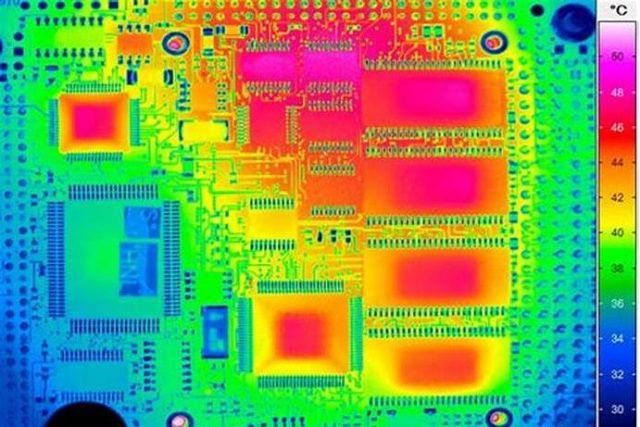
Yield, Reliability & Hidden Risks
Fine line PCBs introduce several risks if not properly controlled:
- Open Circuits:
Trace breaks due to over-etching - Short Circuits:
Insufficient spacing leads to bridging - Signal Variability:
Minor geometry changes affect impedance - Electromigration Risk:
Higher current density in narrow traces - Long-Term Reliability Issues:
Thin conductors are more sensitive to thermal stress
In high-reliability applications, these risks must be carefully evaluated.
Cost vs Density: Finding the Balance
Fine line technology directly impacts cost:
Cost Drivers:
- Advanced imaging (LDI)
- Tight process control
- Lower manufacturing yield
- Increased inspection requirements
Engineering Trade-Off:
- Finer lines → higher density
- Finer lines → higher cost & risk
Smart approach:
Use fine line only where necessary, not across the entire design.
When Should You Use Fine Line PCB?
Use fine line PCBs when:
- Routing between fine-pitch BGA pads
- High pin count designs exceed standard routing capacity
- Space constraints are critical
- HDI structures alone are not sufficient
Avoid when:
- Standard trace/space meets requirements
- Cost sensitivity is high
- Manufacturing capability is limited
Final Thoughts
Fine line PCBs represent the edge of PCB manufacturing capability, enabling designers to achieve extreme density and compact layouts.
However, success depends on:
- Aligning design with real manufacturing limits
- Applying disciplined design rules
- Balancing density with yield and reliability
At KKPCB, we support fine line PCB projects with advanced LDI technology, precision etching control, and strong DFM collaboration, ensuring your designs are not only dense—but also manufacturable and reliable.
