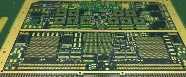
A High Layer Count PCB is a printed circuit board with 8 or more signal layers, often extending to 20–40 layers or more in advanced systems. These boards enable dense routing, compact design, and integration of multiple high-speed and RF circuits in a single assembly.
High layer count PCBs are critical in:
-
High-performance computing
-
Networking and data center equipment
-
Aerospace and defense electronics
-
RF and high-speed digital systems
By increasing the number of layers, engineers can optimize signal routing, improve power distribution, and reduce board size while maintaining signal integrity.
Design Advantages
High layer count PCBs offer several key benefits:
-
High-Density Routing:
Multiple signal and power planes allow complex interconnects without increasing PCB footprint. -
Improved Signal & Power Integrity:
Dedicated power and ground planes reduce impedance discontinuities and minimize crosstalk. -
Compact Design:
Stacking layers enables integration of more functionality in smaller spaces, critical for modern electronics. -
Enhanced Thermal Management:
Internal planes and copper pours provide heat dissipation paths for high-power circuits. -
Flexibility in Stack-Up Configuration:
Engineers can separate analog, digital, RF, and high-speed layers to optimize performance.
Engineering Challenges
Despite advantages, high layer count PCBs present significant challenges:
-
Stack-Up Complexity:
Layer sequencing, plane symmetry, and signal routing require precise planning to avoid interference and maintain impedance. -
Manufacturing Tolerances:
Tight control over lamination, via alignment, and material thickness is essential to prevent warping or delamination. -
Signal Integrity Concerns:
High-speed traces require careful routing, controlled impedance, and minimal layer transitions to reduce reflection and insertion loss. -
Cost and Yield:
Increased layer count raises manufacturing cost and risk of yield loss, requiring careful quality control. -
Thermal Stress:
During soldering and operation, thermal expansion must be carefully managed to maintain reliability.
Fabrication & Quality Assurance
Producing high layer count PCBs involves advanced manufacturing processes:
-
Lamination:
Multiple layers are bonded under precise temperature and pressure to maintain flatness and alignment. -
Via Technology:
Blind, buried, and through vias connect internal and external layers while maintaining signal integrity. -
Copper and Surface Finishes:
Optimized copper weight, ENIG, hard-gold, or immersion silver finishes ensure durability and high-speed performance. -
Testing:
-
Impedance and continuity testing
-
X-ray and AOI inspections for layer alignment and via integrity
-
Thermal cycling to verify long-term reliability
-
High-speed signal validation for SI and PI compliance
-
KKPCB applies these fabrication and QA techniques to deliver high layer count PCBs with consistent electrical and mechanical performance.
Applications
High layer count PCBs are widely used in:
-
High-Performance Computing: CPUs, GPUs, and server motherboards
-
Networking Equipment: High-speed routers, switches, and data centers
-
Aerospace & Defense Electronics: Avionics, radar, and satellite systems
-
RF & Microwave Modules: Antennas, filters, and transceivers
-
Industrial Automation: Complex sensor networks and robotic control systems
By combining advanced multilayer design, precise fabrication, and rigorous quality control, KKPCB ensures High Layer Count PCBs meet the demanding requirements of modern high-speed, high-density electronic systems.
