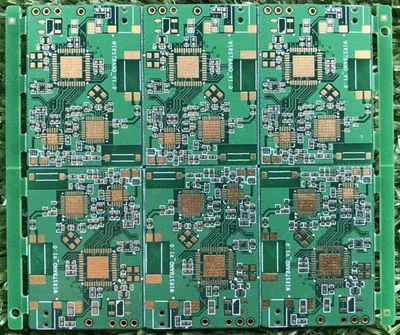
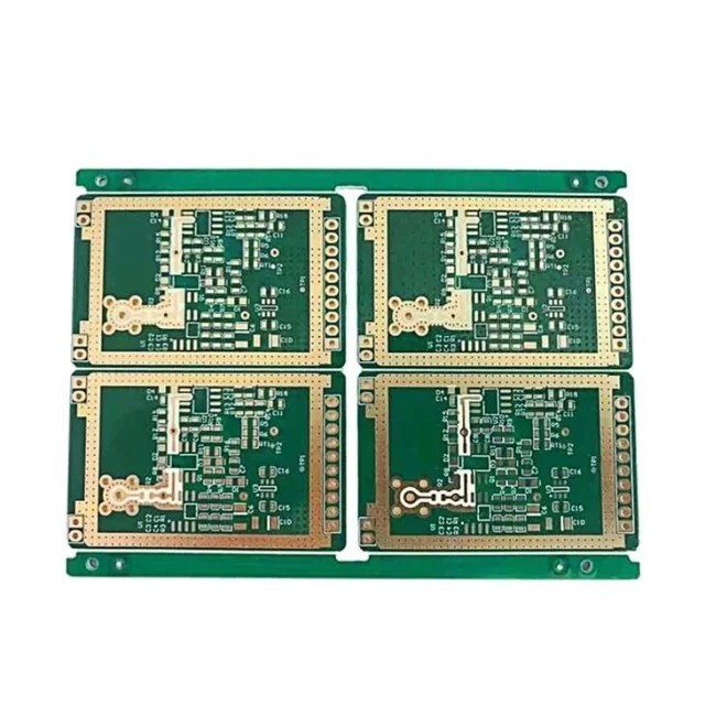
An RO4350B PCB is a printed circuit board built using Rogers RO4350B laminate, a widely adopted high-frequency material known for its low dielectric loss, stable dielectric constant (Dk ≈ 3.48), and excellent thermal reliability.
Unlike traditional PTFE-based materials, RO4350B is a hydrocarbon ceramic laminate, which combines high-frequency performance with easier manufacturability similar to standard FR-4 processes. This makes it a cost-effective solution for RF and high-speed digital applications.
RO4350B PCBs are commonly used in:
-
RF and microwave circuits
-
Wireless communication systems (5G, Wi-Fi, LTE)
-
Automotive radar and ADAS modules
-
High-speed data transmission systems
Material Advantages
RO4350B offers a unique balance between performance and manufacturability:
-
Low Loss Performance:
With a low dissipation factor (Df ≈ 0.0037 at 10 GHz), RO4350B minimizes signal attenuation, making it suitable for high-frequency designs. -
Stable Dielectric Constant:
The Dk remains consistent across a wide frequency range, enabling accurate impedance control and predictable signal behavior. -
Thermal Reliability:
A low coefficient of thermal expansion (CTE) and high glass transition temperature improve stability during thermal cycling and soldering processes. -
FR-4 Compatible Processing:
Unlike PTFE materials, RO4350B can be processed using conventional PCB fabrication techniques, reducing production complexity and cost.
Design Considerations
Designing RO4350B PCBs requires attention to both RF performance and manufacturability:
-
Controlled Impedance:
Precise trace width, spacing, and substrate thickness are essential for maintaining impedance in RF and high-speed circuits. -
Trace Geometry Optimization:
Short signal paths, smooth bends, and minimal via transitions reduce insertion loss and reflections. -
Layer Stack-Up Planning:
Multilayer designs often combine RO4350B with FR-4 in hybrid stack-ups to optimize cost and performance. -
Grounding and Shielding:
Continuous ground planes and via stitching improve EMI suppression and signal integrity. -
Thermal Design:
Thermal vias and copper planes help dissipate heat in high-power RF components.
Fabrication & Reliability
RO4350B PCBs benefit from streamlined manufacturing but still require precision control:
-
Drilling & Plating:
Standard mechanical drilling can be used, but tight tolerance control ensures minimal impedance discontinuities. -
Lamination:
RO4350B laminates bond well in multilayer structures, especially in hybrid stack-ups with FR-4. -
Surface Finishes:
ENIG, immersion silver, or hard gold finishes are selected based on RF performance and durability requirements. -
Quality Assurance:
-
Impedance testing for RF traces
-
Vector Network Analysis (VNA) to evaluate insertion and return loss
-
AOI/X-ray inspection for multilayer and via integrity
-
Thermal stress testing to validate long-term reliability
-
KKPCB applies strict fabrication controls to ensure RO4350B PCBs deliver consistent electrical and mechanical performance.
Applications
RO4350B PCBs are widely used in high-frequency and high-reliability systems:
-
Wireless Communication: RF front-end modules, antennas, and base stations
-
Automotive Radar Systems: 24 GHz and 77 GHz radar modules for ADAS
-
Aerospace & Defense Electronics: High-frequency communication and radar systems
-
High-Speed Networking: Data transmission boards requiring low loss and stable impedance
-
Test & Measurement Equipment: RF diagnostic and calibration systems
By combining low-loss performance, stable dielectric properties, and manufacturability advantages, KKPCB delivers RO4350B PCBs that meet the demands of modern RF and high-speed electronic applications.
